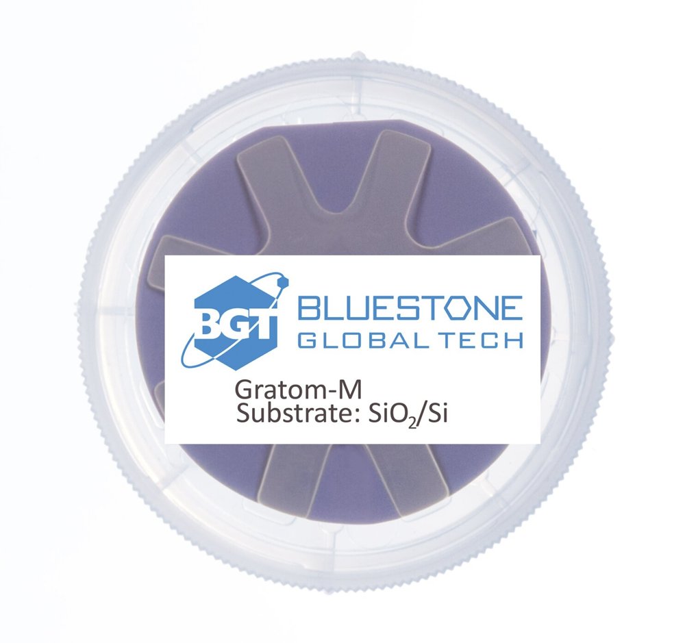
Isolated single graphene domain Large graphene domain (30 – 200 µm) Average Raman Id/Ig < 5% within domain Available Sizes: 2” wafer Wafer spec: thermal grown 285-nm SiO2 on p-type Si substrate (resistivity <0.005 ohm-cm)
Graphene film coverage 95% with occasional holes and cracks (< 5 %) Monolayer graphene percentage 95% of cracks or holes larger than 3 mm: 0 Average Raman Id/Ig < 5% within domain Average Hall mobility of 2000-4000 cm 2/Vs at n=1e12 /cm 2 Average sheet resistance of 300-600 ohm/sq. Available Sizes: 1cm x 1cm, 2” or 4” wafer Wafer spec: thermal grown 285-nm SiO2 on p-type Si substrate (resistivity <0.005 ohm-cm)
CATEGORY
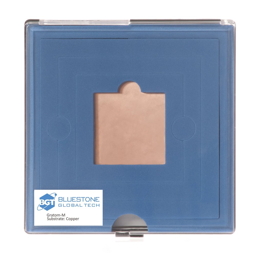
Monolayer percentage 95% Optical transmittance at 550 nm 97% (excl. substrate) Average Raman Id/Ig < 5% within domain Average Hall mobility of 2000-4000 cm 2/Vs at n=1e12 /cm 2 Average sheet resistance of 300-600 ohm/sq. Available Sizes (in 2): 2 x 2, 4 x 4, 8 x 10, 12 x 14 Copper thickness 1mil (25 µm)
CATEGORY
Monolayer with occasional multilayer islands Optical transmittance at 550 nm 95% (excl. substrate) Average sheet resistance of 300-600 ohm/sq. Available Sizes (in 2): 8 x 10, 12 x 14 Copper thickness 1mil (25 µm)
CATEGORY
