By CubeFabs
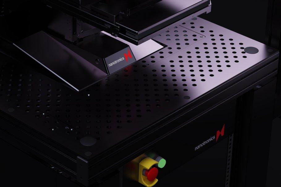
Learn how the nSpec LS can efficiently increase yields and scale processes Benefits Accelerate research with advanced inspection Reduce operational costs nSpec LS allows operators to identify, classify, and assign causality to defects in order to prevent down-line issues. Increase production output Early detection allows manufacturers to produce high yields and scale processes quickly. Features The ideal system for research & development settings Defect inspection is crucial to scaling next-generation devices. The LS system has a small footprint and is used to identify, classify, and assign causality to defects before you scale to volume production. Flexible software User-friendly software makes configuring recipes simple. As needs evolve, recipes are easily saved and modified. Robust hardware The nSpec LS can manage various sample form factors and can inspect a wide variety of new and novel materials. Powered by AI nTelligence is trained to identify early process defects before scaling to high-volume manufacturing. Modular design Easily upgrade the nSpec LS to a PS system when your process is ready to be scaled to volume production. Find device-killing defects. Tech Specs System - Weight: 240 kg - Dimensions (W x D x H): 165 cm x 157 cm x 194 cm - Min. Vacuum Requirement: -21 in.Hg (-70 kPa) - Power Supply: 208—240 VAC, 15A, 50—60 Hz Optics - Illumination Modes: Brightfield, Darkfield, Automated DIC (Nomarski) - Light Source: White light LED (other options available) - Objectives: 5x (included), 1.25x, 2x, 2.5x, 10x, 20x, 50x - Objective Turret: 5-position, User-selectable Stage - Travel, typical: 200 mm X and Y directions - Positioning: Linear servo motors with closed-loop encoders (50 nm resolution) - Repeatability: +/-0.5 µm - Travel Flatness: 30 µm - Centered Load Capacity: 2.27 kg Options - Supported Protocols: SECS/GEM - Illumination: Transmitted light with automated polarizer - Filters: 12-position filter wheel - Machine learning: Offline workstation, nTelligence™, Gen-V-AI Applications Automate inspection across your R&D and production lines. Automated Optical Inspection (AOI) is one of the most efficient forms of device inspection, but it is typically limited by resolution. Our AI detection algorithms overcome this and detect defects that would otherwise go unnoticed.
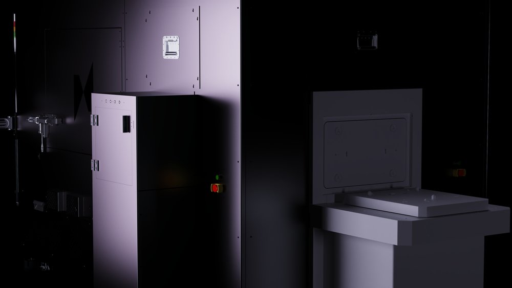
The nSpec TURBO is the ideal system for fully automated high volume manufacturing environments. Benefits Larger efficiency gains when scanning large format samples Flexible handling nSpec TURBO can be built with different configurations to accommodate multiple handling ports and a variety of sample sizes. Reduce operational costs nSpec TURBO allows operators to identify, classify, and assign causality to defects in order to prevent down-line issues. nSpec satisfies a capability need for capturing high-resolution optical photos of wafers at intermediate stages of semiconductor process. nSpec is a versatile and dependable tool that can handle over-one-hundred products. Fit your footprint nSpec TURBO is available in two sizes to speed up quality control on production lines for 300mm sample sizes up to 650mm. Materials Find device-killing defects. Tech Specs nSpec TURBO System - Weight: 1200 kg - Dimensions (W x D x H): 240 cm x 194 cm x 262 cm - Min. Vacuum Requirement: -21 in.Hg (-70 kPa) - Power Supply: 208-240 VAC, 15A, 50-60 Hz - Min. Clean Dry Air: 60 PSI (415 kPa) Optics - Illumination Modes: Brightfield, Darkfield, Automated DIC (Nomarski) - Light Source: White light LED (other options available) - Objectives: 5x (included), 1.25x, 2x, 2.5x, 10x, 20x, 50x - Objective Turret: 5-position, User-selectable Stage - Travel, typical: 350 mm X and Y directions - Positioning: Linear servo motors with closed-loop encoders (50 nm resolution) - Repeatability: +/-2 µm - Travel Flatness: 20 µm - Centered Load Capacity: 12.5 kg Options - Supported Protocols: SECS/GEM, E-84 Interface - Illumination: Transmitted light with automated polarizer - Filters: 12-position filter wheel - Enclosure: CleanCube, Light Curtains - Handling: OCR (frontside or backside), Ergonomic cassette loader, Sample specific fixtures - Load Port: N2 Purge Load Port, 200 mm cassette adapter for Load Port - Machine learning: Offline workstation, nTelligence™, Gen-V-AI Applications Automate inspection across your R&D and production lines Automated Optical Inspection (AOI) is one of the most efficient forms of device inspection, but it is typically limited by resolution. Nanotronics AI detection algorithms overcome this and detect defects that would otherwise go unnoticed.
CATEGORY
The nSpec PRISM offers a complete solution for compound semiconductor front-end wafer manufacturing. Benefits Photoluminescence inspection for front-end wafer manufacturing Process agnostic Gather valuable data points throughout production of compound semiconductors from unpolished substrates to epitaxy and device manufacturing. Advanced illumination The PRISM system incorporates a variety of illumination wavelengths to image a variety of materials and classify multiple defect types. Features The ideal system for compound semiconductors Flexible software User-friendly software makes configuring recipes simple. As needs evolve, recipes are easily saved and modified. Robust hardware The nSpec PRISM can manage various sample form factors and uses Nanotronics' custom illuminator to inspect a wide range of materials. Powered by Nanotronics AI nTelligence is trained to identify early process defects before scaling to high-volume manufacturing. Various lighting modalities The illuminator enables operators to utilize existing imaging modalities while adding UV and IR Illumination to inspection processes. Materials Find device-killing defects. Tech Specs nSpec PRISM Compare with other nSpec products System Weight 363 kg Dimensions (W x D x H) 236 cm x 157 cm x 194 cm Min. Vacuum Requirement -21 in.Hg (-70 kPa) Power Supply 208—240 VAC, 15A, 50—60 Hz Optics Illumination Modes Brightfield, Darkfield, Automated DIC (Nomarski), Ultraviolet Photoluminescence Light Source White light LED, Reflected UV LED (other options available) Objectives 5x (included), 1.25x, 2x, 2.5x, 10x, 20x, 50x Objective Turret 5‑position, User‑selectable Stage Travel, typical 200 mm X and Y directions Positioning Linear servo motors with closed‑loop encoders (50 nm resolution) Repeatability +/-0.5 µm Travel Flatness 30 µm Centered Load Capacity 2.27 kg Wafer Loader Cassette 25 wafers / cassette, single Standard H‑Bar Standard Wafer Sizes 50, 75, 100, 125, 150, and 200 mm Wafer Alignment Automatic by notch or flat Options Supported Protocols SECS/GEM Illumination Transmitted light with automated polarizer Filters 12‑position filter wheel Enclosure CleanCube (included) Handling OCR (frontside or backside), Ergonomic cassette loader, Sample specific fixtures Machine learning Offline workstation, nTelligence™ Applications Automate inspection across your R&D and production lines Automated Optical Inspection (AOI) is one of the most efficient forms of device inspection, but it is typically limited by resolution. Nanotronics AI detection algorithms overcome this and detect defects that would otherwise go unnoticed.
CATEGORY
The nSpec PS is highly flexible and detects defects on a variety of wafers, substrates, and materials. Benefits Unparalleled automation for optical inspection in production settings Reduce operational costs nSpec PS allows operators to identify, classify, and assign causality to defects in order to prevent down-line issues. Increase production output Early detection allows manufacturers to produce high yields and scale processes quickly. Features The ideal system for production settings Flexible software User-friendly software makes configuring recipes simple. As needs evolve, recipes are easily saved and modified. Robust hardware The nSpec PS can manage various sample form factors and uses Nanotronics' custom illuminator to inspect a wide range of materials. Powered by Nanotronics AI nTelligence is trained to identify early process defects before scaling to high-volume manufacturing. Clean environment Upgrade the nSpec PS to include CleanCube, a modular clean environment that protects components from contaminants. Materials Find device-killing defects. Tech Specs System - Weight: 363 kg - Dimensions (W x D x H): 236 cm x 157 cm x 194 cm - Min. Vacuum Requirement: -21 in.Hg (-70 kPa) - Power Supply: 208—240 VAC, 15A, 50—60 Hz Optics - Illumination Modes: Brightfield, Darkfield, Automated DIC (Nomarski) - Light Source: White light LED, (other options available) - Objectives: 5x (included), 1.25x, 2x, 2.5x, 10x, 20x, 50x - Objective Turret: 5-position, User‑selectable Stage - Travel, typical: 200 mm X and Y direction - Positioning: Linear servo motors with closed‑loop encoders (50 nm resolution) - Repeatability: +/- 0.5 µm - Travel Flatness: 30 µm - Centered Load Capacity: 2.27 kg Wafer Loader - Cassette: 25 wafers / cassette, single Standard H-Bar - Standard Wafer Sizes: 50, 75, 100, 125, 150, and 200 mm - Wafer Alignment: Automatic by notch or flat Options - Supported Protocols: SECS/GEM - Illumination: Transmitted light with automated polarizer - Filters: 12‑position filter wheel - Enclosure: CleanCube - Handling: OCR (frontside or backside), Ergonomic cassette loader, Sample specific fixtures - Machine learning: Offline workstation, nTelligence™ Applications Automate inspection across your R&D and production lines Automated Optical Inspection (AOI) is one of the most efficient forms of device inspection, but it is typically limited by resolution. Nanotronics AI detection algorithms overcome this and detect defects that would otherwise go unnoticed.
CATEGORY
CubeFabs are AI-operated, modular, prefabricated semiconductor fabs. These fabs are designed to be cost and time efficient to build, and reconfigurable for different materials and manufacturing processes. CubeFabs use proprietary AI process control to scale difficult to manufacture and defect prone materials like Gallium Oxide, unlocking major efficiency gains over silicon for data centers and EV infrastructure. Pre-fab architecture sets a new standard for factory build times and allows site owners to expand capacity with additional fabs. CubeFabs can monitor production and self-improve in real time. Our patented AI platform, nControl™, automates, monitors, and corrects highly complex manufacturing processes in real-time. Each deployment follows local guidelines and regulations. Because the materials being produced are efficient, few resources are needed and very little waste is produced. Designing a semiconductor fabrication facility with easy access to local greenery is healthy for the engineers and the ecosystem.
CATEGORY
