By MEMSIC Inc.
High Performance Low Power Hall-Effect Sensor MHA18x Series FEATURES - Low power CMOS process - Wide operation voltage range: 1.65~5.5V - Ultra-low power consumption, <5uA@1.8V - Good RF noise immunity - -40 C to +85 C operation - RoHS compliant APPLICATIONS - TWS headset - Smart meter - Cover switch - Domestic appliances - Laptop - Industry DESCRIPTION Figure 1: Signal Path Devices List Devices: MHA182AS-S, Package: SOT553, Polarity: Single output S unipolar, Output: push pull, ESD-HBM: ±3.5KV, Quantity / Reel: 3000 Devices: MHA183AS, Package: SOT23-3L, Polarity: Single output Omnipolar, Output: push pull, ESD-HBM: ±4.5KV, Quantity / Reel: 3000 SPECIFICATIONS (Measurements @ 25 C, unless otherwise noted; V DD =1.8V unless otherwise specified) Supply Voltage (V DD ): Min 1.65, Typ 1.8, Max 5.5 V Supply Current: Min 2.5, Typ 5.0 μA Supply Current (-40~85 C): Min 2.5, Max 10.0 μA Power Down Current: 1.0 nA Operating Temperature: Min -40, Max 85 C Storage Temperature: Min -55, Max 125 C Awake Tim (T awake ): Min 50, Typ 100 μs Period (T period ): Min 50, Typ 100 ms Duty Cycle: 0.05 % Output High (V OH ) IOUT =+0.5mA: Min VDD -0.3, Typ VDD -0.1, Max VDD +0.1 V Output Low (V OL ) IOUT =-0.5mA: Min -0.3, Typ 0.1, Max 0.3 V Output Current: Min -0.5, Max 0.5 mA Sampling Frequency: 20 Hz Magnetic Opening Point (B OP ): Min 27, Typ 37, Max 47 Gauss Magnetic Releasing Point (B RP ): Min 17, Typ 27, Max 37 Gauss Hysteresis Window (B HYS ): Min 3, Typ 10, Max 17 Gauss SOT23 PIN DESCRIPTION Pin NO. 1, Pin name VDD, Description: Power supply Pin NO. 2, Pin name OUT, Description: S or N pole detection output Pin NO. 3, Pin name GND, Description: Ground SOT553 PIN DESCRIPTION Pin NO. 1, Pin name NC Pin NO. 2, Pin name GND, Description: Ground Pin NO. 3, Pin name NC Pin NO. 4, Pin name VDD, Description: Power supply Pin NO. 5, Pin name OUT, Description: S or N pole detection output THEORY OF OPERATION This Hall switch is fully integrated CMOS IC. It output high-low signal following magnetic field changing. Normally it works with a magnet and detect the magnet close and away. Figure 5: Hall Effect Figure 6: Output signals of OUTN and OUTS pins Figure 7: Output signals Omnipolar OUT pins Figure 8: Sensor and magnet Figure 9: Field by magnet (different size and distance) Magnetic flux density SOLDER REFLOW PROFILE 1. Reflow is limited by 2 times. Second reflow should be applied after device has cooled down to room temperature (25 ℃). 2. Recommended reflow profile for Pb free process is shown in Figure 3. The time duration of peak temperature (260 ℃) should be limited to 10 seconds. 3. Type 4 solder paste is recommended for a better SMT quality. Figure 10: Recommended solder reflow profile MANUAL SOLDERING 1. Soldering/repairing MHA18x manually via solder iron or heater gun is not recommended. 2. Avoid bending or torqueing the PCB after the sensor is assembled. SOT23 PACKAGE OUTLINE DIMENSION Unit: mm 2.926±0.1 1.626±0.1 2.800±0.2 1.900±0.1 Max 1.250 1.100±0.1 0.650 0.150 0.405 0.400 0.59 10° ±2° 12° ±2° 4°Ref 0.170±0.03 Figure 13: Mechanical package outline dimensions Notes : a) Sensitive area located at the center of package within 0.3mm diameter circle. b) Unless otherwise specified, Tolerances is ±0.05mm. SOT23 PACKAGE TAPE AND REEL PACKING Products are put into carrier tape according to package type. The quantity for each full reel is 3000pcs per reel with 7” lock reel. Please refer to below Figure Details for tape and reel packing as below: a) Tape and reel carriers are in accordance with ANSI/EIA-481 b) Tape and reels are NOT designed to be baked at high temperatures c) Each tape and reel is typically dry packed in a moisture barrier bag (MSL1). Section A-A Section B-B 8.00 1.75 3.50 Lead: 300mm Tail: 500mm R0.50 4.00 3.30 3.20 5.50 Carrier tape Cover tape φ1.55 0.25 3.20 2.55 1.47 5° MAX 5° MAX 0.60 5° MAX 3.30 R0.30 R0.30 User direction of unreeling BBAA Figure 14: Carrier tape dimension and device orientation SOT553 PACKAGE OUTLINE DIMENSION Unit: mm Figure 15: Mechanical package outline dimensions Notes : c) Sensitive area located at the center of package within 0.3mm diameter circle. d) Unless otherwise specified, Tolerances is ±0.05mm. SOT553 TAPE AND REEL Products are put into carrier tape according to package type. The quantity for each full reel is 3000pcs per reel with 7” lock reel. Please refer to below Figure Details for tape and reel packing as below: a) Tape and reel carriers are in accordance with ANSI/EIA-481 b) Tape and reels are NOT designed to be baked at high temperatures c) Each tape and reel is typically dry packed in a moisture barrier bag (MSL1). Figure 16: Carrier tape dimension and device orientation
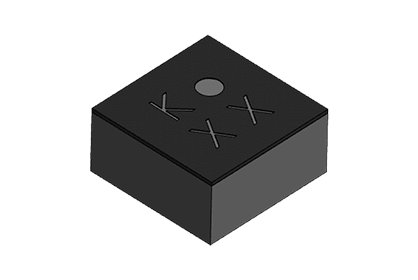
WLP package, 0.85x0.85x0.4mm, I²C/I³C interface, ±30g range, high performance AMR Magnetometer Application: Smart Phone/Pad/NoteBook; Wearable Device; Smart Home; Smart Device Monolithic integrated 3-axis AMR magnetic sensor and electronic circuits requiring fewer external components Superior Dynamic Range and Accuracy ±30 G FSR 20bits operation mode 0.0625mG per LSB resolutio 2 mG total RMS noise Enables heading accuracy of ±1º Sensor true frequency response up to 1KHz Ultra-Small Wafer Level Package 0.8x0.8x0.4mm On-chip automatic degaussing with built-in SET/RESET function Eliminates thermal variation induced offset error (Null field output) Clears the residual magnetization resulting from strong external fields On-chip sensitivity compensation On-chip temperature sensor Selftest signal available Dataready Interrupt (I³C only) Low power consumption 1µA power down current I²C slave, FAST (≤400 KHz) mode I³C interface, Compatible with MIPI I³C pecfication version 1.0 1.62V to 3.6V wide range single power supply 1.2V compatible I²C interface 1.8V 1.8V compatible I³C interface RoHS complian
CATEGORY
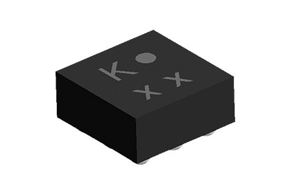
BGA package, 1.2x1.2x0.5mm, I²C interface, ±30g range, high performance AMR Magnetometer Application: Wearable Device, Smart Home, Smart Device Fully integrated 3-axis magnetic sensor and electronic circuits requiring fewer external components Superior Dynamic Range and Accuracy ±30G FSR with 16bits operation 1mG per LSB resolution 2mG total RMS noise Enables heading accuracy of 1º Output data rate up to 600 Hz Ultra Small Low profile package 1.2x1.2x0.5mm Degaussing with built-in SET/RESET function Eliminates thermal variation induced offset error (Null field output) Clears the residual magnetization resulting from strong external fields On-chip sensitivity compensation On-chip temperature sensor MotionDetection and DataReady Interrupt Low power consumption 1µA power down current I²C Slave, FAST (≤400 KHz) mode 1.8V single low power supply compatible Low to 1.2V I²C interface RoHS compliant
CATEGORY
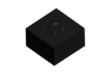
BGA package, 1.6x1.6x0.6mm, multiple I²C device addresses, I²C interface, ±16g range, high performance AMR Magnetometer Fully integrated 3-axis magnetic sensor and electronic circuits requiring fewer external components Superior Dynamic Range and Accuracy ±16G FSR with 16/14bits operation 0.5mG/2mG per LSB resolution in 16/14bits operation mode 1.5mG total RMS noise Enables heading accuracy of ±1º Max output data rate of 800 Hz (12 bits mode) Ultra Small Low profile package 1.6x1.6x0.6mm Allows for elimination of temperature variation induced offset error (Null field output) Clears the sensors of residual magnetization resulting from strong external fields On-chip sensitivity compensation Low power consumption (140µA @ 7Hz ) 1µA (max) power down function I²C Slave, FAST (≤400 KHz) mode 1.62~3.6V wide power supply operation supported, 1.8 V I/O compatibility RoHS compliant
CATEGORY
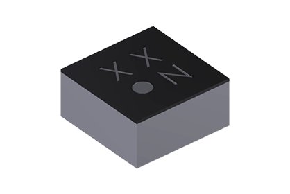
WLP package, 0.8x0.8x0.4mm, I²C interface, ±30g range, high performance AMR Magnetometer Monolithic integrated 3-axis AMR magnetic sensor and electronic circuits requiring fewer external components Superior Dynamic Range and Accuracy ±30G FSR 20bits operation mode 0.0625mG per LSB resolution 2mG total RMS noise Enables heading accuracy of 1º Sensor true frequency response up to 1KHz Ultra-Small Wafer Level Package 0.8x0.8x0.4mm On-chip automatic degaussing with built-in SET/RESET function Eliminates thermal variation induced offset error (Null field output) Clears the residual magnetization resulting from strong external fields On-chip sensitivity compensation On-chip temperature sensor Selftest signal available Low power consumption 1µA power down current I²C slave, FAST (≤400 KHz) mode 1.62V to 3.6V wide range single power supply 1.2V logic IO RoHS compliant
CATEGORY
