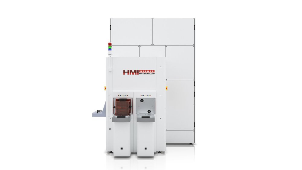
By ASML
The eScan 600 is a highly flexible e-beam wafer inspection system that can operate in multiple modes, allowing chipmakers to capture the widest variety of defect types in a single system. Together with a high throughput and superfine detection resolution, this versatility helps cut the cost of chip R&D and ramp-up. Versatility The eScan 600 can be used for physical defect inspection, voltage contrast defect inspection and material contrast defect inspection in backscattered electron (BSE) mode. This means that patterning defects, electrical defects (including open, short and leakage defects) and material contrast defects can be detected with just one system. Sensitivity The eScan 600 offers extremely high defect detection resolution to identify sub-design rule patterning defects. For instance, it can detect physical defects just a few nanometers in size, enabling efficient R&D for the most advanced microchips. In addition, GDS (graphic design system) assisted features such as GDS pattern-of-interest and GDS binning use design information to enhance defect sensitivity and classification. The eScan 600 can also be connected to SuperNova to support online die-to-database (D2DB) inspection, which uses additional design information to further improve sensitivity. Throughput The eScan 600 includes a number of features to increase the inspection throughput. Our patented technology enables a uniquely large field of view (120 µm x 120 µm) to increase throughput in leap-and-scan mode without harming sensitivity. The continuous scan mode provides high throughput inspection for voltage contrast and larger physical defects, while the SkyScan mode allows millions of patterns-of-interest in pre-identified locations to be scanned in just a few hours.

High NA EUV lithography system. High NA EUV is the next step in our constant pursuit of shrink. Like NXE systems, it uses EUV light to print tiny features on silicon wafers. And by turning the NA knob, we deliver even better resolution: The new platform, known as EXE, offers chipmakers a CD of 8 nm. That means they can print transistors 1.7 times smaller – and therefore achieve transistor densities 2.9 times higher – than they can with NXE systems. The headline advance in High NA EUV lithography is the new optics. The ‘NA’ in the name refers to numerical aperture – a measure of the ability of an optical system to collect and focus light. And it’s called High NA EUV because we’ve increased the NA from 0.33 in our NXE systems to 0.55 in EXE systems. The higher NA is what gives the systems their better resolution. Implementing this increase in NA meant using bigger mirrors. But the bigger mirrors increase the angle at which light hit the reticle, which has the pattern to be printed. At the larger angle the reticle loses its reflectivity, so the pattern can’t be transferred to the wafer. This issue could have been addressed by shrinking the pattern by 8x rather than the 4x used in NXE systems, but that would have required chipmakers to switch to larger reticles. Instead, the EXE uses an ingenious design: anamorphic optics. Rather than uniformly shrinking the pattern being printed, the system’s mirrors demagnify it by 4x in one direction and 8x in the other. That solution reduced the angle at which the light hit the reticle and avoided the reflection issue. Importantly, it also minimized the new technology’s impact on the semiconductor ecosystem by allowing chipmakers to continue using traditionally sized reticles. Because of their anamorphic optics, EXE systems have exposure fields half the size of their NXE predecessors. It therefore takes twice as many exposures to pattern a single wafer. Twice as many exposures could have meant twice as long to print a wafer. Instead, we took it as a challenge. The solution? Much faster wafer and reticle stages. The wafer stage in an EXE system accelerates at 8g, twice as fast as the NXE’s wafer stage. And the EXE’s reticle stage accelerates four times faster than the NXE’s – 32g, the equivalent of a race car going from 0 to 100 km/h in 0.09 seconds. With its new stages, the TWINSCAN EXE:5000 can print more than 185 wafers per hour, an increase compared to the NXE systems already being used in high-volume manufacturing. And we have a roadmap for increasing that to 220 wafers per hour in 2025. This productivity was key to making sure the integration of High NA into chip fabs was economically viable for chipmakers. High NA EUV lithography will enable chipmakers to print the smallest features on the most advanced microchips. But in the meantime, chipmakers haven’t just been waiting around. They’ve found other ways to get around the resolution limitations of their lithography systems by using more complicated production processes. These workarounds come at a cost. They increase production time and provide additional opportunities to introduce defects that could affect the chip’s performance. With its CD of 8 nm, the EXE:5000 enables chipmakers to simplify their manufacturing processes. The result? More cost-efficient production of advanced microchips. The EXE:5000 represents an evolution of EUV lithography, not a revolution. We’ve reused as much of our existing EUV technology as possible and changed only those aspects necessary to deliver the system’s resolution and productivity enhancements. And, like our NXE EUV systems, EXE systems are made up of modules that can be independently tested before being integrated into a complete system. Why did we prioritize commonality and modularity throughout our EUV lithography systems? Because that way all of our systems benefit from lessons learned over 20 years of EUV development. Using tried-and-tested technology reduces the risk of things going wrong. And the modules streamline the system’s installation and integration into a customer fab. That means the systems will start producing chips more quickly – our customers will start their R&D in 2024–2025 and move into high-volume manufacturing in 2025–2026. The 8 nm resolution of the EXE:5000 means that chipmakers can pack more transistors into a single chip. Smaller transistors are more energy efficient – that means the chips will be able to do more with less. So the tiny features printed by the EXE:5000 will form the foundation of the most advanced microchips. And, because of the system’s productivity, chipmakers can manufacture these chips in huge numbers.
CATEGORY

ASML's YieldStar systems do just what their name suggests: they help our customers increase their yield, or the proportion of functioning chips on the wafer. YieldStar allows manufacturers to track key production parameters such as overlay (the accuracy with which two layers of a chip are aligned). Our YieldStar systems are usually integrated into the production line so that they can measure quickly and accurately, looping the data back to the lithography system for real-time corrections to the manufacturing process. Diffraction YieldStar is a diffraction-based optical metrology system which applies the simple fact that an object’s shape determines how light reflects from it. For example, shine a beam of light onto a repeating pattern of lines on a wafer, and you can easily predict what the resulting pattern of scattered light should look like. If you collect the scattered light using a high-resolution digital camera, you can quickly determine how well the prediction matches reality and thus how well the pattern of lines has been printed. Fast, accurate wafer metrology In wafer metrology, key manufacturing parameters such as overlay (the accuracy with which two layers of a chip are aligned) and focus (how sharp the image is) are monitored by measuring how well a particular repeating pattern (the ‘metrology target’) is printed on the wafer. These measurements are made at marked locations across the wafer. Integrated into the production line Prior to YieldStar, wafers were taken out of the production line to be measured manually. By integrating our solution into the production line (or ‘track’), chipmakers can now use YieldStar to gather their metrology data quickly and accurately, offering better control over their production processes. Metrology data is analyzed using control software and fed back to the lithography system in real-time, enabling customers to tune the manufacturing process further for optimal yield. From repeating patterns to real structures Our latest developments in diffraction-based metrology feature new optics technologies to generate more accurate data, faster, measuring thousands of data points for each batch of wafers. YieldStar matches the productivity of our lithography systems for wafer-to-wafer control on the most advanced chip nodes. Additionally, YieldStar is used for after-etch metrology to inspect actual device structures with more accuracy and higher measuring speeds than our competitors’ scanning electron microscope (SEM) solutions.
CATEGORY
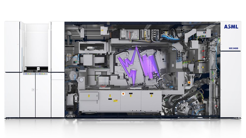
Built on the future-proof NXT4 platform, our TWINSCAN NXT:2050i pushes overlay limits and offers unparalleled productivity for an immersion lithography system. The TWINSCAN NXT:2050i is where state-of-the-art immersion lithography system design meets advanced lens design with a numerical aperture (NA) of 1.35 – the highest in the semiconductor industry right now. This step-and-scan system is a high-productivity, dual-stage tool designed for volume production. By combining high productivity with unprecedented overlay performance, this system addresses multiple patterning requirements, providing a cost-effective solution for the manufacturing of 300 mm wafers at advanced Logic and DRAM nodes. 01. Productivity The TWINSCAN NXT:2050i is raising the game for semiconductor productivity, able to produce 295 wafers per hour. This system is able to deliver 400 to 500 additional wafers per day, by reducing overhead times compared to earlier TWINSCAN systems. The redesigned wafer stage features a more powerful motor, able to accelerate faster and perform movements even more accurately. The TWINSCAN NXT:2050i features a new immersion hood that reduces water loss, significantly improving defectivity performance. This translates to improved product yield and higher productivity through fewer slowdowns. 02. Optics This system features a 1.35 NA 193 nm catadioptric projection lens that can achieve production resolutions down to 40 nm (C-quad) and 38 nm (dipole) and an in-line design supporting full 26 x 33 mm field size, 4X reduction and reticle compatibility with existing designs. The lens elements of this system are equipped with manipulators to correct for optical aberrations, enabling maximum productivity for low-k 1 imaging. The lens fingerprint is now optimized in high-density and can be matched towards EUV. The Parallel ILIAS (PARIS) sensor allows for a parallel measurement of optical aberrations throughout the projection slit, thus enabling a more accurate alignment, enhanced reticle heating correction and on-the-fly lens heating correction. The PARIS sensor used by the TWINSCAN NXT:2050i features an improvement in the sensor mount that translates to better positioning reproducibility. 03. Imaging performance This system delivers improved cross-matching performance with our extreme ultraviolet (EUV) NXE systems. It can achieve a 2.5 nm cross-matching on product overlay. The reticle stage is equipped with enhanced clamps, improving not only the reliability of the system but also the overlay. The ORION alignment sensor, which offers increased accuracy of alignment measurements and enhanced process robustness, is future upgradable to 12 color mode. The level sensor (UVLS-2) uses ultraviolet light to minimize the system’s sensitivity to process stack variations during in-line mapping of the wafer surface. The sensor has an increased measurement density which allows for greater leveling accuracy at the edge of the wafer.
CATEGORY
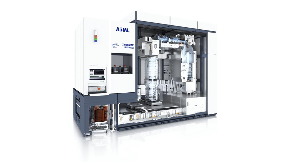
Like the TWINSCAN NXT:2000i, this step-and-scan system is a high-productivity, dual-stage immersion lithography tool designed for volume production of 300 mm wafers at advanced nodes. By combining high productivity and excellent image resolution with unprecedented overlay and focus performance, the TWINSCAN NXT:1980Di addresses multiple patterning requirements and thus provides our customers with a cost-effective solution for advanced nodes. 01. Productivity In this system, novel gas lifetime extensions reduce machine downtime and reinforce proven 6 kHz ArF laser technology to provide high power to support high throughput. Immersion hood design improvements widen the window to optimize defectivity using low contact angle resists without topcoat. Together with the TWINSCAN NXT:1980Di maintenance scheduler, a comprehensive service package optimizes system availability by taking advantage of system idle time to perform required routine maintenance. 02. Optics The TWINSCAN NXT:1980Di includes a 1.35 NA 193 nm catadioptric projection lens that can achieve production resolutions down to 40 nm (C-quad) and 38 nm (dipole) and an in-line design supporting full 26 x 33 mm field size, 4X reduction and reticle compatibility with existing designs. Lens elements are equipped with manipulators to correct for optical aberrations, thus enabling maximum productivity for low-k1 applications. The FlexRay Prepared Illuminator allows maximum flexibility by extending the range of conventional and off-axis illumination to enable advanced pupil shaping for low-k1 imaging. 03. Imaging performance The NXT:1980Di can achieve a ≤ 1.6 nm single-machine (dedicated chuck) full-wafer-coverage overlay, and a ≤ 2.5 nm matched-machine (to reference wafer) full-wafer-coverage overlay, thanks to improved wafer table flatness and wafer load grid, as well as improvements to the grid setup and layout-dependent grid calibration.These improvements also allow for better focus control. The system’s Parallel ILIAS (PARIS) sensor allows customers to make parallel measurements of optical aberrations throughout the projection slit, which enables more accurate alignment, improved reticle heating correction and on-the-fly lens heating correction. Finally, the SpotLess 2 Wafer Table Cleaning System automatically cleans excessive focus spots caused by particles on the exposure chuck without the intervention of an operator.
CATEGORY
