By Eulitha AG
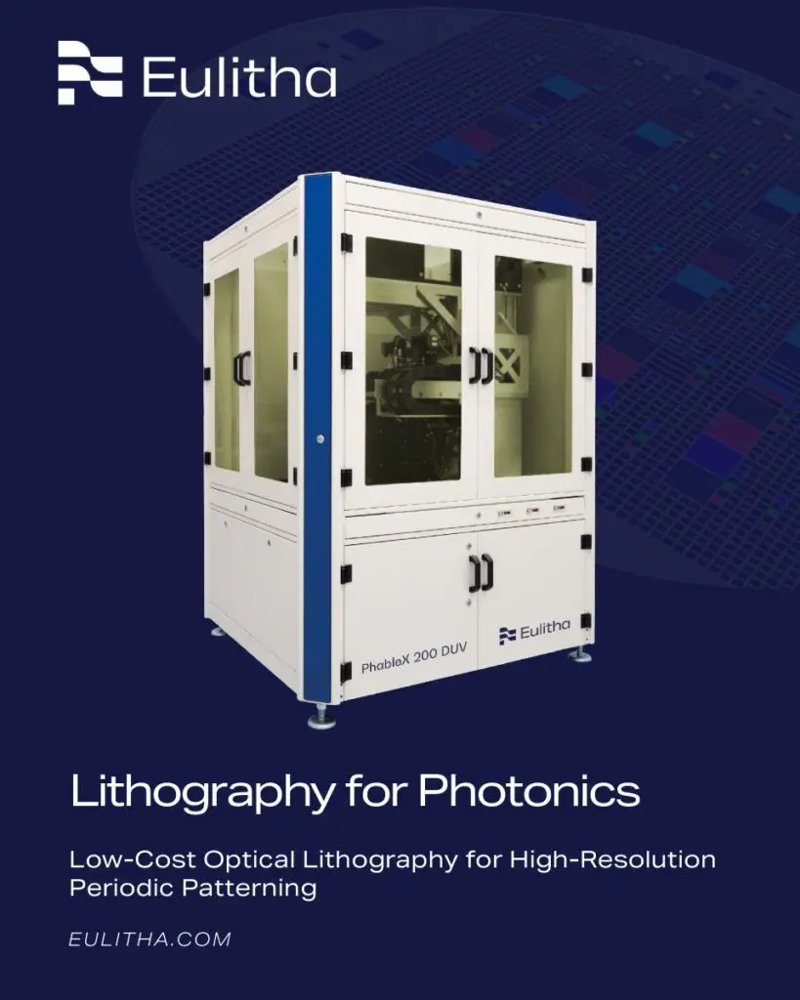
Eulitha's tool platforms use proprietary non-contact optical lithography technology, known as displacement Talbot lithography (DTL), to deliver a range of advantages. High-resolution, precision patterning is ideal for advanced VCSEL arrays, while its large exposure field covers an entire 6-inch wafer in a single shot, reducing stitching errors and enhancing uniformity. The system supports high-throughput production with consistent results across wafers and production batches. A key feature of DTL is the large depth of focus (DOF), which allows for patterning on non-flat wafers. Together, these capabilities lead to higher device performance, tighter process control, and reduced cost per die for manufacturers. Asian VCSEL Foundries Select Eulitha's Lithography Tool for 6-Inch Production as Market Demand Grows "Our PhableX systems are enabling our customers in Asia to scale up their 6-inch VCSEL production with confidence, delivering the precision and productivity needed to address growing demand in critical sectors like LiDAR and optical interconnects."
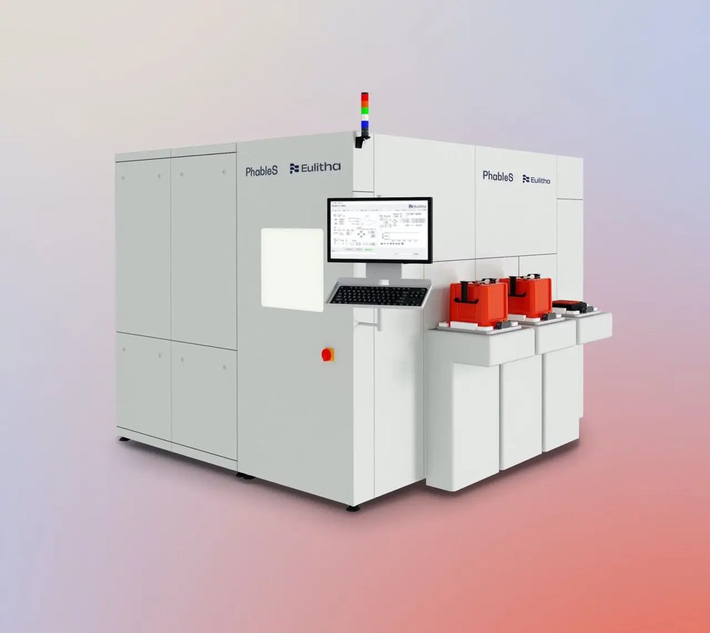
Step-and-repeat lithography system The PhableS is a step-and-repeat lithography tool designed for larger wafer sizes, such as 200 mm, 300 mm, and beyond. Using the large exposure fields of displacement Talbot lithography (DTL), the PhableS tool can fill larger substrates with multiple exposures. This tool is equipped with automated wafer and mask handling within a particle-controlled environment, ideal for high-volume industrial production. It features a variable exposure field size, allowing selective printing across multiple device masks. Specifications - Resolution (linear grating): UV <125 nm half-pitch; DUV <65 nm half-pitch - Wafer size: 300 mm; larger size on request - Mask format: 6″ - Illumination uniformity: <3% - Resist thickness: UV 1 µm; DUV 0.1 µm - Operation: Automated wafer and mask handling, factory interface compatible - Overlay alignment: <1 µm frontside, < 5µm backside - Duty cycle control: Variable compatible; At 150 nm pitch: 0.4 to 0.65 DC At 300 nm pitch: 0.3 to 0.75 DC - Throughput: 40 WPH - Maximum Exposure Field Size: 140 mm x 140 mm
CATEGORY
