TFCompanion software has an option to correct for high NA effects (Fig. 4). TFCompanion has an option to set NA of the measurement in Advance Tab (main screen) – this will include NA correction in the calculations during the curve fitting (for FFT correction is normally not needed)
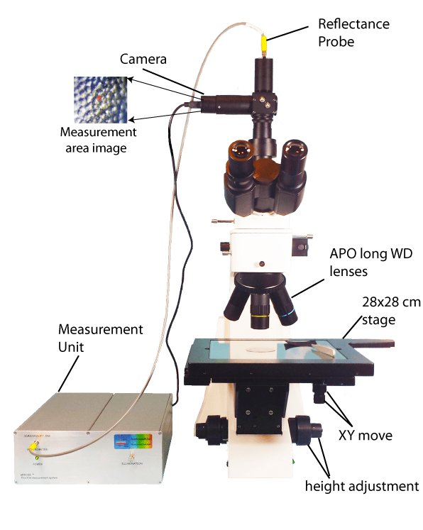
MProbe 40 measures film thickness and refractive index in small spot with one mouse click. Microspectrophotometer(MSP) combines the power and capability of an inspection type microscope and MProbe measurement unit in a fully integrated system for film thickness measuremnt in small spot. It is used for thousands of applications worldwide and a complete line of standard models is available support them. The thicknesses from 1nm to 2mm, including multilayer filmstacks, can be measured quickly and reliably. Different models are distringuished primarily by wavelength ranges and resolutions of spectrometers, which in turn determined the thickness range that can be measured. Film thickness measurement in small spot is used in several types of applications: - on cylindrical or curved surfaces – syringes, stents, pins, wires, etc. A small spot creates a flat field to achieve accurate measurement even on a highly curved surface - non-uniform, rough coatings or light scattering material like high haze or nanoparticles infused films. Small spot localize the measurement and minimize the effects of light scattering and non-uniformity - patterned wafers, MEMS and other application requiring high lateral resolution / measurement in small areas. Long working distance objectives (95 mm parfocal length) are used for comfortable and reliable measurement. Large selection of Visible, NIR and UVVisNIR achromatic objectives is available, depending on application requirements. WHY MPROBE 40? - Flexible modular system: select the best configuration for your application. - Precision: unmatched precision <0.01nm or 0.01% - Materials: 500+ extended material database - Software: user friendly and feature rich TFCompanion software can handle even most complex applications.No limit on number of layers, support for backside reflectance, surface roughness, dullness and much more. - Integrated camera and imaging software allows to pinpoint measurement location and display results directly on the image - Affordable: unmatched price/performance WHAT IS IN THE BOX - Main unit (includes spectrometer, light source) - Upright inspection microscope accessory with adapter, 50W TH illuminator, 2MB CMOS camera and 4 objectives turret (one LWD objective included) - Fiberoptics reflectance probe - TFCompanion -RA software, USB dongle(license key), USB memory stick with softwar distribution,User Guide and other materials - Calibration set (bare Si wafer and/or Quartz plate and/or Al mirror) depending on the model and black absorber - Test sample 200nm Si oxide or PET film, depending on the model - USB cable (for connecting main unit to PC) - 24VDC power supply adapter (110/220V) BASIC SPECIFICATION: Precision: <0.01nm or 0.01% (s.d.of 100 measurements on 200nm oxide) Accuracy: <1nm or 0.2% (filmstack dependent) Stability:< 0.02nm or 0.2% Spot size: 4μm to 200μm (typical- depending on objective used) Sample size: up to 200 mm Options: -XY Mapping stage: XY motorized mapping stage with controller ans mapping software support. 150x150mm and 200x200mm options. Step size: 0.5 μm; Repeatability: 1μm. Replacing standard manual microscope stage (275mmx 275) with fine and quick adjustment that is included by default – Visible and Vis-NIR LWD objectives: -2x lens (200μm measurement) -10x lens (40μm measurement) -20x lens (20μm measurement) -50x lens (8μm measurement) -100x lens (4μm measurement) spot sizes listed for standard 400μm fiberoptics. Visible lens: 430nm -900nm wavelength range; VisNIR lens: 450-1700nm wavelength range. Standard LWD parfocal 95mm lenses, mounting thread M26x36TPI (like Mitutoyo) are compatible – All mirror achromatic objectives: All mirrors Cassegrain objectives: -10x objective -15x objective -20x objective. LWD 95mm parfocal objectives with mounting thread M26x36TPI. Fully covers UVVisNIR system wavelength range:190-1700nm
CATEGORY
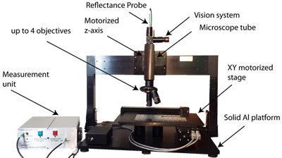
MProbe 60 is a complete turnkey system designed for R&D centers and small manufacturing. It combines the ability to measure thickness/n&k with mapping automation and small spot measurement. MProbe 60 is used by leading R&D/Nanotechnology centers worldwide. The thicknesses from 1nm – 2mm, including multilayer filmstacks, can be measured quickly and reliably. Different MProbe 40 models are distringuished primarily by wavelength ranges and resolutions of spectrometers, which in turn determine the thickness range that can be measured. WHY MPROBE 60? - A turnkey system with mapping automation that is flexible and modular - Precision: unmatched precision <0.01nm or 0.01% - Materials: 500+ extended material database - Software: user friendly and feature rich TFCompanion software can handle even most complex applications.No limit on number of layers, support for backside reflectance, surface roughness, dullness and much more. Integrated camera and imaging software allows to pinpoint measurement location and display results directly on the image - Affordable: unmatched price/performance MPROBE 60 Series: Thickness ranges WHAT IS IN THE BOX - Main unit (includes spectrometer, light source) - Solid platform with motorized mapping stage and controller - Microscope tube on z-axis motorized stage or a bracket with standard lens (depending on configuration) - Fiberoptics reflectance probe - TFCompanion -RA software, USB dongle(license key), USB memory stick with software distribution,User Guide and other materials - Calibration set (bare Si wafer and/or Quartz plate and/or Al mirror) depending on the model and black absorber - Test sample 200nm Si oxide or PET film, depending on the model - USB cables and 24VDC power supply adapters (110/220V) BASIC SPECIFICATION: Precision: <0.01nm or 0.01% (s.d.of 100 measurements on 200nm oxide) Accuracy: <1nm or 0.2% (filmstack dependent) Stability:< 0.02nm or 0.2% (daily measurements for 20 days) Spot size: 4μm to 200μm (typical- depending on objective used) Sample size: up to 300 mm Mapping stage: 0.5 μm resolution, 1μm repeatability Z-axis: 0.25 μm resolution, 0.5μm repeatability OPTION / DESCRIPTION / COMMENTS -XY Mapping stage: XY motorized mapping stage with controller ans mapping software support. 150x150mm, 200x200mm and 300x300mm option. Step size: 0.5 μm; Repeatability: 1μm. One of the stage has to be selected. – Transmission option: Attachment to support transmittance measurement. Includes: quartz stage insert, fiberoptics, collimator optics and 45 deg. mirror cube. Optics matching wavelength range of the main system – Visible and Vis-NIR LWD objectives: -2x lens (200μm measurement) -10x lens (40μm measurement) -20x lens (20μm measurement) -50x lens (8μm measurement) -100x lens (4μm measurement) spot sizes listed for standard 400μm fiberoptics. Visible lens: 430nm -900nm wavelength range. VisNIR lens: 450-1700nm wavelength range. Standard LWD parfocal 95mm lenses, mounting thread M26x36TPI (like Mitutoyo) are compatible – All mirror achromatic objectives: All mirrors Cassegrain objectives: -10x objective -15x objective -20x objective. LWD 95mm parfocal objectives with mounting thread M26x36TPI. Fully covers UVVisNIR system wavelength range:190-1700nm MPROBE 60 MODEL / Wavelength range, nm / Description / Thickness range / Comments MPROBE VIS-MAP: 400-1000nm; F4 Spectrometer,3600 pix CCD, 16 bit ADC, 5W Tungsten-Halogen lamp; 10nm – 75 μm; Spot size down to 2μm possible with 100x objective and 200μm core fiberoptics MPROBE UVVISSR-MAP: 200nm -1100nm; F4 Spectrometer, 2048 pix (backthinned),16 bit ADC 20W TH lamp, 30W Deuterium short-ark lamp; 1nm -75μm; Spot size down to 20μm possible with 40x all reflective objective and 400μm fiberoptics MPROBE VISHR-MAP: 700nm -1100nm; F4 Spectrometer, 2048 pix (backthinned),16 bit ADC, 5W TH lamp; 1μm-400μm; Spot size down to 2μm possible with 100x objective and 200μm fiberoptics MPROBE NIR-MAP: 900nm-1700nm; F4 spectrometer, InGaAs detector 512 pix., 16 bit ADC, 5W TH lamp; 50nm – 85μm; Spot size down to 2μm possible with 100x objective and 200μm core fiberoptics MPROBE UVVISNIR-MAP: 200nm -1700nm; F4 Spectrometer, 2048 p ix (backthinned),16 bit ADC 20W TH lamp, 30W Deuterium short-ark lamp. F4 spectrom eter, InGaAs detector 512 pix., 16 bit ADC, 5W TH lamp; 1nm -85μm; Spot size down to 20μm possible with 40x all reflective objective and 400μm fiberoptics MPROBE NIRHR-MAP: 1500nm – 1550nm; F4 spectrometer, InGaAs detector 512 pix., 16 bit ADC, 5W TH lamp or SLD option; 10μm-1800μm (glass) 4μm-400μm (Si); Spot size down to 2μm possible with 100x objective and 200μm core fiberoptics
CATEGORY
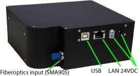
ARIEL: COMPACT ASTIGMATISM-CORRECTED SPECTROMETER Solid metal construction for mechanical and thermal stability. Footprint: 144x133mm, height:55mm,weight: 800 g Ariel is a fiberoptics spectrometer for industrial and R&D desktop applications.It uses unfolded Czerny-Turner system with 80mm optical benchand torroid mirror for astigmatism correction.Spectrometer fiberoptics input is SMA 905. Gigabit LAN and USB 2 connections and extensive auxilary port functions for communication with other devices. It is a rugged spectrometer with fixed optical bench without moving or adjusting parts. Ariel fiberoptics spectrometer has low aberration design for the full spectrum. The spectrum has clean symmetrical peaks and improved sensitivity at short and near-infrared wavelengths. All this coupled with fast integration time, onboard signal conditioning and LAN connectivity make Ariel spectrometer perfectly suited for industrial and R&D applications. Czerny Turner unfolded design with torroid mirror reduces light scattering, corrects astigmatism and optimized for low abberation and flat field across all measured spectrum ARIEL SPECTROMETER: BASIC SPECIFICATION VIS /VisX: Wavelength range, nm: 380nm -1000nm; 450nm-1050nm (VisX); Wavelength resolution (with 20µm slit): 1nm; Dynamic range: 5000; Minimum integration time: 10 µs; Onboard data conditioning: Averaging, boxcar, nonlinearity correction, dark signal correction, fixed pattern noise correction; Detector: CMOS, 2048 pixels; Optical system: Unfolded Czerny-Turner, fixed; Optical bench: 80 mm; Diffraction grating: 400 g/mm, blazed at 500nm; Astigmatism correction: Torroid mirror; Input fiber connector: SMA 905; F: 3; ADC: 16 bits, 10 MHz; Connection: Gigabit LAN, USB 2.0; Auxiliary port: 4xGPIO, I2C, 2xSPI, 4xPWM, 4xDAC, trigger, strobe; Power: 24VDC UVVIS: Wavelength range, nm: 200nm -1000 nm; Wavelength resolution (with 20µm slit): 1nm; Dynamic range: 5000; Minimum integration time:.10 µs; Onboard data conditioning: Averaging, boxcar, nonlinearity correction, dark signal correction, fixed pattern noise correction; Detector: CMOS, 2048 pixels; Optical system: Unfolded Czerny-Turner, fixed; Optical bench: 80mm; Diffraction grating: 300 g/mm dual-blazed; Astigmatism correction: Torroid mirror; Input fiber connector: SMA 905; F: 3; ADC: 16 bits, 10 MHz; Connection: Gigabit LAN, USB 2.0; Auxiliary port: the same; Power: 24VDC Imaging (detector) plane of spectrometer with and without astignatism correction. A. Ariel spectrometer B. Same design w/o astigmatism correction. C. Design with 600 g/mm (typical for small spectrometers) w/o astigmatism correction Astigmatism correction: Spherical mirrors spectrometers can have significant astigmatism that is not corrected by Czerny-Turner design. Astigmatism means that a point at the entrance slit becomes a line at the imaging plane (on the detector). This results in the loss of light and increased scattering potential. Essentially, in case of oblique incidence, spherical mirror has different focus in sagittal and tangential planes. Astigmatism can be corrected using a cylindrical lens or torroid mirror. Torroid mirror is a cleaner but more expensive solution. This correction increases light collection 4x-5x. It also decreases the coma across the spectrum – this is important for clean symmetrical peaks in spectroscopic data. NonLinearity correction: CMOS detector response is fairly linear at the low signals (<50% of dynamic range). But becomes non-linear at higher signals. The non-linearity is caused by the source- follower and charge to voltage converting capacitor. Hence, nonlinearity is slightly different from pixel to pixel. It is accurately corrected by factory calibration. The residual non-linearity is < 0.5% Dark signal correction: Dark signal depends on integration time and temperature. For an active CMOS detector, each pixel has a bit different dark current with a different rate of change. Each spectrometer is carefully calibrated on per pixel basis and for range of operating temperatures. This calibration is stored on board and automatically loaded depending on temperature of the detector. This way, the dark is fully corrected. Typical nonlinearity of the detector pixel: original and corrected Typical dark signal vs. integration time for detector pixel
CATEGORY
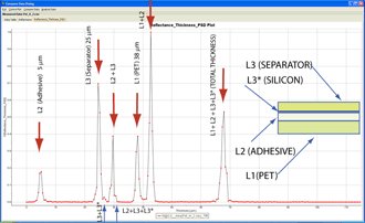
TFCOMPANION SOFTWARE:REFLECTANCE, TRANSMITTANCE, ELLIPSOMETRY TFCompanion software is included with all MProbe systems. It is also available as a standalone software for thin-film data analysis (various versions for reflectance, ellipsometry, imaging ellipsometry, etc.) Software plays a critical role in thin-film thickness measurement. It has two distinct functions that are transparent to the user: control/data acquisition of reflectance data( from the hardware) and data analysis/interpretation. TFCompanion is a powerful and user friendly software application for thin film analysis and metrology.It combines versatile analytical tools for interpretation of measurement data – to determine actual physical parameters of a filmstack (like thicknesses of the layers and optical properties of the materials). Analyze: Reflectance, transmittance, ellipsometry spectra together or separately. Supports analysis of Imaging ellipsometry, reflectance, transmittance data. Determine filmstack parameters based on measurement results: thickness, optical constants, surface roughness, bandgap… Simulate: reflectance/transmittance/ellipsometry spectra from a specified filmstack, determine measurement sensitivity to filmstack parameters Estimate: measurement repeatability based on selected filmstack and system configuration. Pre-flight optimization of measurement recipe for maximum precision. Includes Large materials library(500+ materials), supports large number of parametrized material types from Cauchy to Tauc-Lorentz to Drude approximations to represent optical constants dispersion for a wide variety of materials and enable n&k measurement. Imports: measurement data in any text format, specifically supports import from all major ellipsometer/reflectomer instruments Integrates: with many commercial fiberoptics spectrometers for smooth data acquisition and data analysis WHY TFCompanion? - User friendly yet powerful software. Build from ground up based on decades of experience in optical methrology - Extended materials database (500+) and support for many parameterized material types (Cauchy,Tauc-Lorentz, etc.) - Support corrections for backside reflectance, focused beam, dullness, suirface roughness, wavelength/angle resolution and many more. - Option for importing and analyzing reflectance, transmittance, ellipsometry data together - Automation: integrated TCPIP Modbus compliant server WHAT IS IN THE BOX - USB dongle (license key). Can be transfered between the computers easily. Does not require driver installation - a memory stick with software distribution and documentation - One year technical support and software updates (after one year, annual subscrition is available) TFCompanion Versions (see brochure for more details): -R supports reflectance/ transmittance data analysis -E supports ellipsometry data analysis -RE supports ellipsometry and Reflectance transmittance data analysis -REI supports ellipsometry, imaging ellipsometry, reflectance & transmittance data analysis -RA advanced version reflectance/transmittance and hardware integration (supplied with MProbe)
CATEGORY
