By Graphenest
Graphene nanoplatelets are integrated directly into standard industrial polymers, delivering consistent electromagnetic shielding and electrical conductivity across high-frequency ranges, without metallic additives, without process overhaul. G-Shield™ is a product line of graphene-based polymer compounds, currently available in PP and PVC bases, built to replace conventional metal shielding with a lighter, processable, and equally effective alternative. Lighter. More flexible. Easier to manufacture. The same shielding performance at a fraction of the weight, fully compatible with extrusion, injection moulding, and 3D printing workflows, and scalable within existing production lines. Suited for cables, electronics packaging, and advanced mobility systems, G-Shield positions graphene as a practical, ready-to-use industrial-grade solution for today's high-performance products.
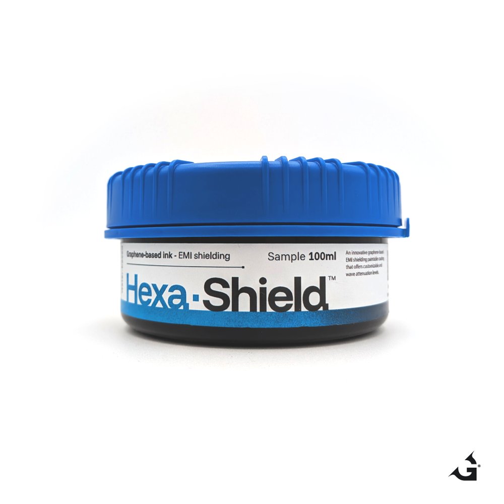
Hexa-Shield is a graphene-based conductive coating formulated for EMI shielding of complex geometries and surfaces. Applied by spray, brush, or bar coating, it provides controlled shielding effectiveness across a broad frequency range. Suitable for electronics enclosures, defence components and industrial substrates. Each order includes a Certificate of Analysis (CoA) and a processed sample (bar-coated). 100 ml – Evaluation Download TDS: Hexa-Shield booklet For bulk or industrial orders, email sales@graphenest.com
CATEGORY
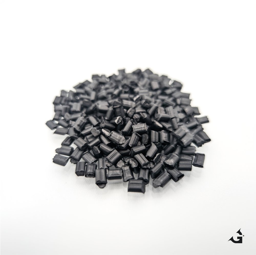
G-Shield/PP is a graphene-based polypropylene compound engineered for effective electromagnetic interference (EMI) shielding. It delivers consistent conductivity and processability in injection moulding and extrusion applications. Suitable for automotive, electronics, and defence components requiring reliable EMI attenuation. Each order includes a Certificate of Analysis (CoA) and a processed sample (injection-moulded plate). For bulk or industrial orders, email sales@graphenest.com
CATEGORY
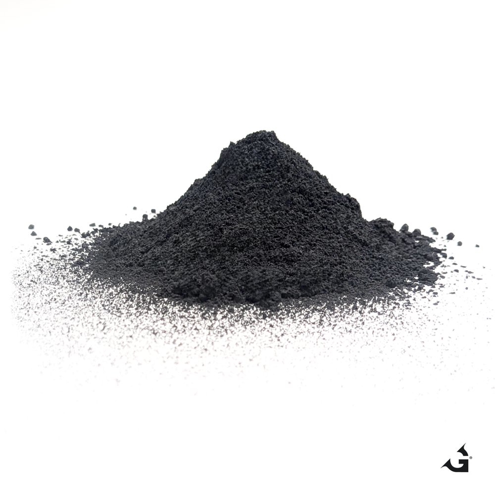
Industrial-grade Graphene Nanoplatelets (GNP) produced via proprietary liquid-phase exfoliation of natural graphite. High aspect ratio and controlled lateral dimensions deliver consistent performance in polymer compounding, coatings, lubricants and energy storage applications. Each order includes a Certificate of Analysis (CoA). 50 g – Lab sample
CATEGORY
G-Prime™ is Graphenest's premium graphene nanoplatelet powder, produced through a proprietary nano-exfoliation process that delivers exceptional cristallinity, consistent particle size distribution, and industry-leading electrical conductivity. Available as dry powder or in custom-made formulations, G-Prime is the raw material that makes advanced products possible. By integrating graphene nanoplatelets directly into standard industrial polymers, G-Prime delivers: Electromagnetic shielding High EMI attenuation performance across a broad high-frequency range Electrical conductivity Consistent surface and volume conductivity without metallic additives Lightweight construction Up to 75% lighter than equivalent metal-based shielding solutions Design flexibility Compatible with extrusion, injection moulding, and 3D printing workflows Scalable processing Drop-in integration into existing polymer manufacturing lines The result is a material platform suited for cables, enclosures, electronics packaging, and advanced mobility systems, where weight reduction, manufacturing simplicity, and shielding performance must coexist. Supply form (powder and custom-made formulations) Graphene nanoplatelets characterization Value range Raman spectroscopy XPS SEM¹ 4 POINT PROBE² Atomic % [C]: 94.27 - 99.62 Peak ratio - ID/IG: 0.06-0.19 Atomic % [O]: 0.32 - 5.59 Peak ratio - I2D/IG: 0.22-0.51 Atomic % [S]: 0.00 - 0.14 Conductivity [S/cm]: 0.52 - 2.60 Atomic % [N]: 0.00 - 0.18 Size (D10) [μm]: 1.46 - 6.00 Size (D50) [μm]: 248.16 - 406.84 Average particle size [μm]: 4.94 - 13.10 Size (D90) [μm]: 2.27 - 7.13 1 Particle size measured using least n100 particles 2 Conductivity of pressed pellet (~520 bar), Ø= 13 mm, thickness ~1mm Product data sheet TEM JEOL 2100 operated at 200 kV Copper TEM grid as sample holder TEM images were collected using a CCD Gatan UltraScan camera and processed with the Gatan software DigitalMicrograph SEM FEI Quanta 650 FEG SEM Images acquired at 10 kV and under high vacuum, using an Everhart Thornley secondary electron detector Low resistivity Si used as substrate RAMAN Witec alpha300 R Confocal Raman Microscope • The system is equipped with a UHTS300 spectrometer coupled to the Andor Peltier cooled CCD detectors • The signal acquisition was performed with a 532 nm excitation line, 100x lens (NA = 0.9) and 600g/mm grating XPS Thermo Scientific ESCALAB 250Xi • Acquisitions under ultra-high vacuum, spectra generated by an Al monochromated X-ray source operated at 15 keV and 200W power • Peak-fitting using Avantage software, with smart-type background subtraction and charge correction to the reference value of adventitious carbon ID/IG = 0.09 I2D/IG = 0.31 Key benefits • Exceptional electrical and thermal conductivity for better performance • Scalable integration into existing manufacturing processes • Enables lighter and more durable materials • Promotes reduced material usage contributing to weight and cost savings • Enhanced sustainability through lower environmental impact
CATEGORY
