By IMT Masken und Teilungen AG
Waveguides with gratings using evanescent field excitation for high-sensitivity sensing platforms Principle of evanescent field sensing using thin film waveguides with sub-micrometric gratings for light coupling. The small extension of the evanescent field above the waveguide allows very high detection sensitivity. Grating Laser Waveguide Applications - Life science sensing applications - Analysis of living molecules in real time Benefits - High quality gratings, excellent homogeneity - Low defect ratio (also for large chip formats) - High repeatability at volume production - Competitive up-front costs - Combination with fluidic channels Technical Data Substrate materials - Schott D263T (or equivalent) - Refractive index: 1.52 at 633 nm - Dimension: 5“ × 5“ × 0.7 mm (or thinner) Waveguide (planar or rib) - Material: Ta 2O5 (or other oxides) - Refractive index: 2.12 at 633 nm - Thickness: 100 - 500 nm - Attenuation: < 3 dB / cm at 532 nm Light coupling grating - Binary phase grating - Period: 300 - 1000 nm - Depth: 10 - 100 nm
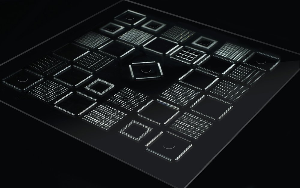
Highly accurate: 2D and 3D calibration plates for automation Calibration plates and dummy chips are important tools for the calibration of optical measurement systems in pick-and-place machines. With their help, the user conducts a machine capability analysis at specified time intervals to determine whether the actual position of the electronic components to be positioned differs from the target position. IMT specialises in the production of large-format substrates between 9 x 9 inches and 32 x 24 inches (228 x 228 mm and 812 x 609 mm), for which it is not possible to use current standard formats. Of course, smaller elements can also be supplied if required by the customer. In other optical systems they are used, for example, as Hartmann plates for the identification of imaging errors in the optical system. Datasheet "Calibration solutions for Pick & Place equipment" Datasheet "Specs for large Calibration Plates" Datasheet "Standard Graticules"
CATEGORY

In the traditional Hartmann test, a pinhole array is positioned in front of the optical system to be investigated. The corresponding 2D point cloud is depicted by the system on a CCD camera. As the pinhole distances on the substrate and the resulting point distances on the CCD are known, it is possible to determine aberrations introduced by the optical system. Shack-Hartmann wavefront sensors use microlenses instead of pinhole arrays. They are generally used in the characterisation of optical systems and in adaptive optics. In ophthalmology, the eyes are measured with a wavefront sensor before laser treatment (LASIK), allowing the areas to be treated to be defined. Customers rely on the ‘Made by IMT’ quality both for Hartmann plates and for the microstructuring of supplied microlens arrays, onto which a metal coating needs to be applied in order to avoid interfering light.
CATEGORY
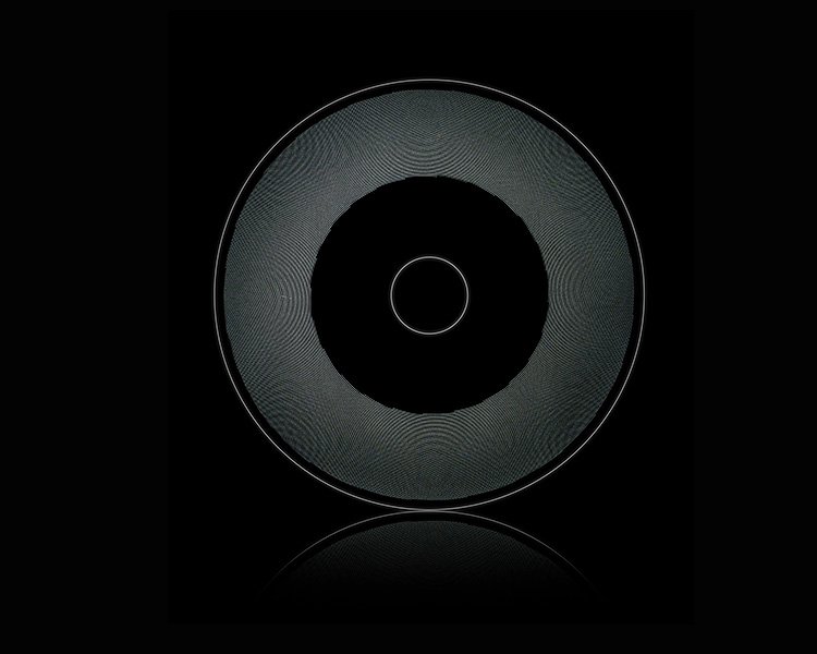
Nipkow discs are used in confocal microscopy. As part of the lighting system, they are also found in fluorescence microscopy and material testing. The elements feature pinholes, which are arranged in a ‘Nipkow pattern’ on a planar substrate. IMT ensures that there are no defects during the microstructuring of the black chrome coating. This is because even the smallest of defects in the size of a pinhole diameter will lead to streaking in the confocal image, thereby rendering the disc unusable.
CATEGORY

Electrophoresis refers, generally speaking, to the movement of charged particles or molecules through an electric field. The speed of the particles is essentially determined by their shape and size. In biochemistry and molecular biology, this relationship is used to separate short and long molecule strands. New lithography processes allow us to combine glass channels with easily accessible gold structures.
CATEGORY
