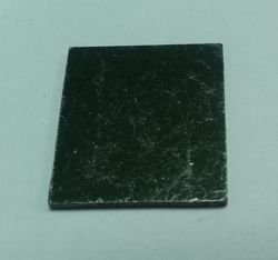
By Nt-mdt
HOPG of the highest quality. Mosaic Spread 0.4 ± 0.1 degrees. Available double- and single-sided. Double-sided HOPG can be used from both sides and its properties are not changed in depth. For one-sided piece the not working side is mat, glare less and can’t be cleaved. The number of working side cleavages of one-sided piece is limited in comparison with double sided substrate. The properties for one-sided piece are changed in depth. €250,00
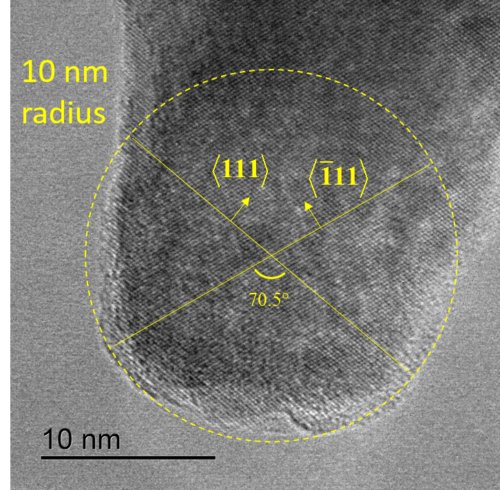
Unique probes with single crystal diamond tip for topography and electrical measurements. Nominal values: force constant -2.8 N/m, resonance frequency –75 kHz. Highly Conductive Long Lasting Sharp Diamond Probes formed by a unique patented process ensure the best possible wear and electrical performance. The tips are sharper and last longer than any other electrical AFM probe. The probes are highly resistant to mechanical destructions and keep their sharpness during the whole working day and more! These probes enable highly repeatable high resolution operation to ensure you consistently get the best possible data from your system. The conductive diamond coating is highly doped with boron which leads to a macroscopic resistivity of 0.003 - 0.005 Ohm•cm. A sharp tip is formed from a single diamond crystal which yields an unsurpassed combination of resolution, mechanical properties and electrical performance. Contact resistance is between 10k and 100k ohms depending on contact radius measured on a silver coated surface. A gold reflex coating is deposited on the detector side of the cantilever to enhance the reflectance of the laser beam. Upon customers' request the next options are available: - super sharp probes with typical curvature radius 2nm; - probes with another lever specification; - probes with individually characterized spring constant and tip radius to enable fully quantitative nanomechanical measurements. Cantilever specifications Geometry: Rectangular Material: Diamond coated Si Cantilever bending: < 3° Bulk tip specifications Si geometry: Rotated (Symmetric) Si tip height (h): 15 ± 2 μm Front angle: 25 ± 2° Back angle: 22 ± 2° Side angle: 18 ± 2° Tip offset: 10 – 20 μm Single crystal diamond tip specifications Geometry: Cone Tip radius: Typical 7nm, guaranteed <10nm Tip height (h): 300 nm ± 100 nm Tilt angle: 0 ± 1° Tip material: Single crystal diamond Highly doped with boron Cone ½ angle: 15 ± 2° General Features Chip size 3.4×1.6×0.3 Reflective side coating Au Tip coating Single crystal diamond, Highly doped with boron Tip curvature radius typical 7nm, guaranteed <10nm Special Features Cantilever series DEP01 Cantilever length, L±10µm: 225 Cantilever width, W±5µm: 35 Cantilever thickness, T±0.5µm: 1.5 Resonant frequency, kHz: min 50, typical 65, max 100 Force constant, N/m: min 1.2, typical 2.8, max 4.5
CATEGORY
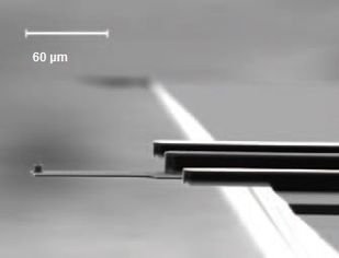
High Aspect Ratio Premium Etalon tips PHANC series, each chip has 2 cantilevers, resonant frequency 235 kHz / 140 kHz, force constant 12 N/m / 3.5 N/m, with Au reflective coating. Premium ETALON tips have conical apex and cylindrical body to minimize tip-related widening of objects investigated. Excellent geometry provides high resolution of AFM scans: - Conical apex of 5-8 nm typical curvature radius and cone angle < 30° suits well for imaging of small objects and nanoparticles; - Narrow cylindrical body with diameter of 300 - 700 nm allows getting detailed images of high objects, making Etalon Premium probes being similar to high aspect ratio probes' models. High Accuracy composite ETALON probes combine the main features allowing to obtain high quality AFM images: - Sharp tip - curvature radius < 10 nm. - Resonance frequency, specified with high accuracy - ±10% within a wafer. - Special chip geometry with vertical sidewalls for convenient operating. - High aspect ratio tip. - Enhanced back-side reflection of the cantilever. - Cost effective price. Specification of PHANC probe series: Material Polysilicon lever, monocrystal silicon tip Chip size 3.6 x 1.6 x 0.4 mm Reflective side Au Cantilever number 2 rectangular Tip shape Cylindrical at the base, conic on the last 1000 nm Tip cone angle φ 30 degrees on the last 1000nm Full tip height ≥8 µm Pedestal/tip ratio 1:1 Tip curvature radius less than 10nm (5-8 nm typically) General Features Material Polysilicon cantilever, silicon tip Chip size 3.6×1.6×0.4mm Reflective side coating Au Tip coating No Tip curvature radius < 10nm Special Features Cantilever series: PHANC Cantilever A: Cantilever length, L±2µm 94; Cantilever width, W±3µm 34; Cantilever thickness, T±0.15µm 1.85; Resonant frequency, kHz min 210, typical 235, max 260; Force constant, N/m min 9, typical 12, max 15 Cantilever B: Cantilever length, L±2µm 124; Cantilever width, W±3µm 34; Cantilever thickness, T±0.15µm 1.85; Resonant frequency, kHz min 125, typical 140, max 155; Force constant, N/m min 2.5, typical 3.5, max 4.5
CATEGORY
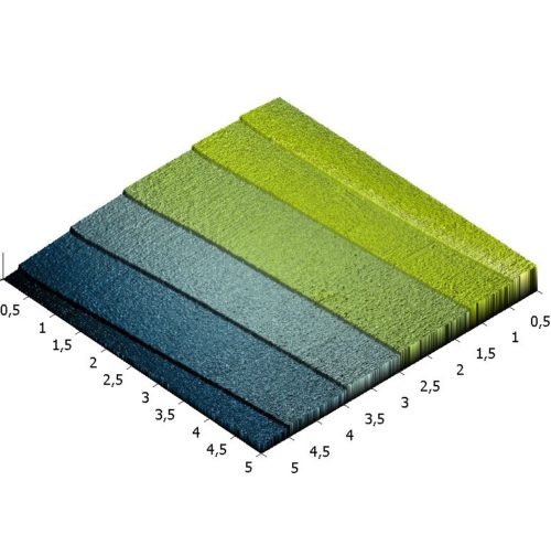
6H-SiC(0001) based calibration sample is designed to perform easy calibrations of AFM scanner vertical movement in several nanometer intervals. The simplicity of calibration process is provided by nearly uniform distribution of monolayer high (1.5 nm) steps on the sample surface demonstrating chemical and mechanical stability. The step height corresponds to the lattice constant of 6H-SiC crystal in [0001] direction. Specification: - Chip size – 5x5x0.3 mm 3 - Average interstep distance – 0.2-0.5 µm - Misorientation of surface ~ 0.3° - Single step height 1.5 nm - Average roughness of the area between steps (terraces) – 0.09 nm Calibration procedure To calibrate AFM scanner movements along the Z axis the following operations are to be performed: - Place the SiC-1.5 nm calibration sample on the flat horizontal working area under the AFM probe. - Approach the AFM probe to the sample surface and make topography scanning in the height measure mode using the scan size of about 10 µm (Fig. 1). Make sure that there is no dust on the surface and choose for further measurements area about to 1.5×1.5 µm 2. - After obtaining good quality AFM-image of the surface area with several steps use the software filter to flatten image so that every single step become horizontal (Fig. 2). Choose the area on AFM-image for obtaining height spectra by using possibilities of AFM software. Please, choose the area with maximum number of steps for better statistics. After obtaining height spectra with peaks corresponding to each step, measure the interpeak distances. Note that distances between neighboring peaks may vary a little (see Fig.3), so it is useful to average distances between peaks by measuring distance between far standing peaks and dividing the measured value by the number of included interpeak distances (A-A on Fig. 3). Change the scanner calibrating constant while average interpeak distance becomes 1.5 nm.
CATEGORY
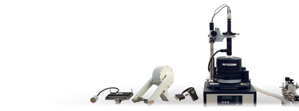
AFM for studies with in-plane and out-plane external magnetic fields Due to the open architecture, the functionality of NTEGRA Aura can be widen essentially: specialized magnetic measurements with external magnetic field (horizontal, up to +/-0.3 T; vertical, up to +/-0.08 T), high-temperature experiments (heating up to 150 °С with temperature maintaining precision of 0.05 °С), etc. SPECIFICATIONS - AFM (contact + intermittent contact) - HybriD mode - Lateral Force Microscopy - Force Modulation Microscopy - Magnetic Force Microscopy - Electrostatic Force Microscopy - Scanning Capacitance Force Microscopy - Kelvin Probe Force Microscopy - Piezoresponce Force Microscopy - Spreading-Resistance Imaging - STM - Nanosclerometry - Lithography: AFM (Force + Current), STM TECHNICAL DATA External magnetic field: Horizontal up to +/-0.3 T; vertical, up to +/-0.08 T Scan type: Scanning by probe Sample size: Up to 100 mm in diameter, up to 15 mm in height Sample weight: Up to 300 g XY sample positiniong range: 5×5 mm Positioning resolution: readable resolution – 5 um; sensitivity – 2 um Scan range: 100x100x10 um Scan range: Up to 200x200x15 um (DualScan mode) Non linearity, XY (with closed loop sensors): ≤0.15% Noise level, Z (RMS in bandwidth 1000 Hz): With sensors 0.06 nm (typically), ≤0.07 nm Noise level, Z (RMS in bandwidth 1000 Hz): Without sensors 0.05 nm Noise level, XY (RMS in bandwidth 200 Hz): With sensors 0.1 nm (typically), ≤0.2 nm Noise level, XY (RMS in bandwidth 200 Hz): Without sensors 0.01 nm Optical viewing system: Optical resolution 3 um; Field of view 2.0-0.4 mm; Continuous zoom available Temperature control: Range From RT to +150 °C; Stability ±0.005 °C (typically), ≤±0.01 °C Vibration isolation: Active 0.7-1000 Hz; Passive above 1 kHz Scanning head can be configured to serve as a stand-alone device for specimens of unlimited sizes. Built-in capacitive sensors have extremely low noise and any area down to 50×50 nm can be scanned with closed-loop control.
CATEGORY
