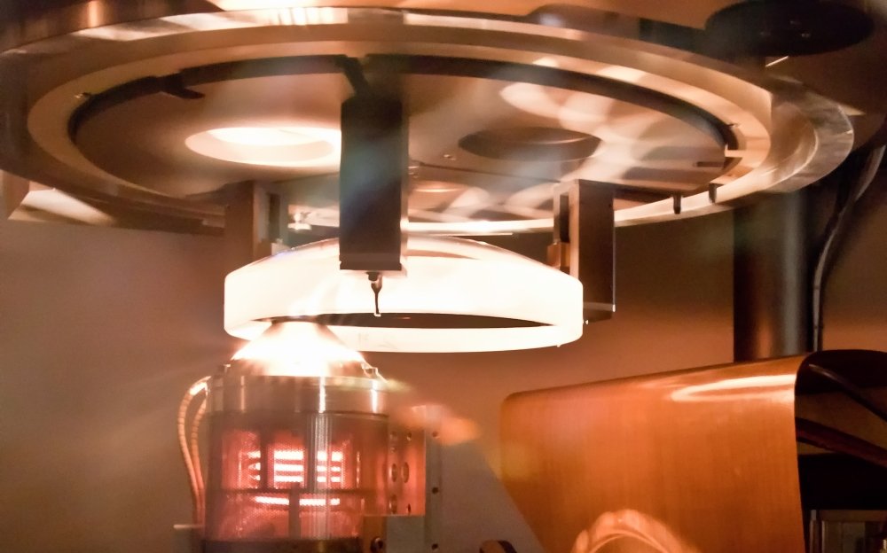
NTG started to develop Ion Beam Figuring plants in 1991 for the nanometer precise correction of surface errors, when only a few people in the world talked about Nanotechnology. IBF IBF(Ion Beam Figuring)-technology is needed when the required quality of the surface can not be achieved by using conventional polishing techniques. Our Customers are the world leader in fabrication of high performance optics. Whereas in the past the use of technology was limited in producing stepper objectives for the semiconductor industry recently we recognize a growing demand of this technology even in the traditional optic industry. R-IBE Pattern transfers into hard materials (glass, …) are more and more of increasing importance. Also in this field NTG can provide a wide spectrum of solutions and Reactive Etching plants. Additionally to the complete Ion Beam Etching and Figuring plants NTG also provides a wide range of accessories for IBF and R-IBE plants such as grid systems, work piece holders, loading and turning devices, sensors,…. Advantages of IBF-technology from NTG - Contactless process – no signs on the surface - no induced stress on the surface - almost any geometry can be treated - large spectrum of processable materials - acquisition costs comparable with MRF plants - low operating costs – no abrasives are necessary – nearly no wearing parts – less cleaning exprenses (for parts and machine) – low maintenance - surface quality PV < λ /10 to λ/20 achievable (depending on the requirements of quality & process speed) - surface quality PV < λ/100, rms < 1nm achievable without additional investments - Know-How resulting of more than 25 years IBF-treatment
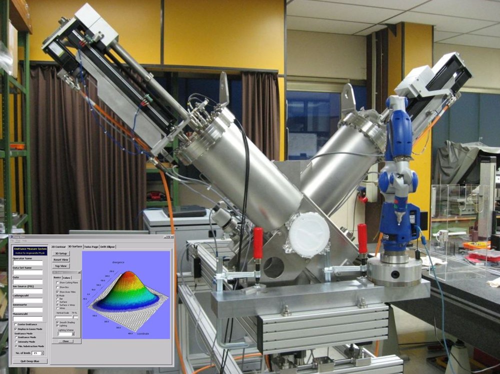
Computer controlled measurement of the emittance and beam profile of an ion beam. The beam emittance analyzer is a “ready to use system” and consists of the following components: Vacuum chamber Slit system Profile grid Precision UHV linear Feedthroughs Electronics Software Computer Graphical display of 2 and 3 dimensional beam emittance, RMS emittance, beam intensity and beam profile. The measurement is based on the slit/harp principle: A profile harp, an array of equidistant metal wires or rods, is placed parallel behind a slit-like aperture. Slit and harp are moved through the beam line transversally. The current induced by the ions, which are hitting the wires, is measured at different positions and for each wire separately. The slit separates such ions of only one certain transversal coordinate (e.g. x). Each wire is located in a certain angle to the slit and hit only by ions with a corresponding angle in their trajectory. The wire-current is proportional to the density of the ions in the phase space element x, x’. Thus each measured value is characterized by three parameters: x, x’, I. An intensity profile of the ion beam in the x, x’-plane is given by a 3-dimensional plot of the current I as a function of x and x’. The area of the x, x’-plane filled by the ion beam is corresponding to its emittance, the so called “total emittance”. Most important value – because of its invariance according to Liouvilles law – is epsilon, the area divided by π. The RMS- and the KV-emittance (KV=RMS4) are calculated with the second momentum of the intensity distribution. The KV-emittance (Kapchinskij-Vladimirskij) is used for the analytical computation of the beam envelope under space charge conditions. The brilliance of the ion beam is a measure by its current density in the transverse 4 dimensional phase space and is calculated by the beam-current divided by the cube of its emittance π², which can be computed either with the total- or with the KV-emittance.
CATEGORY
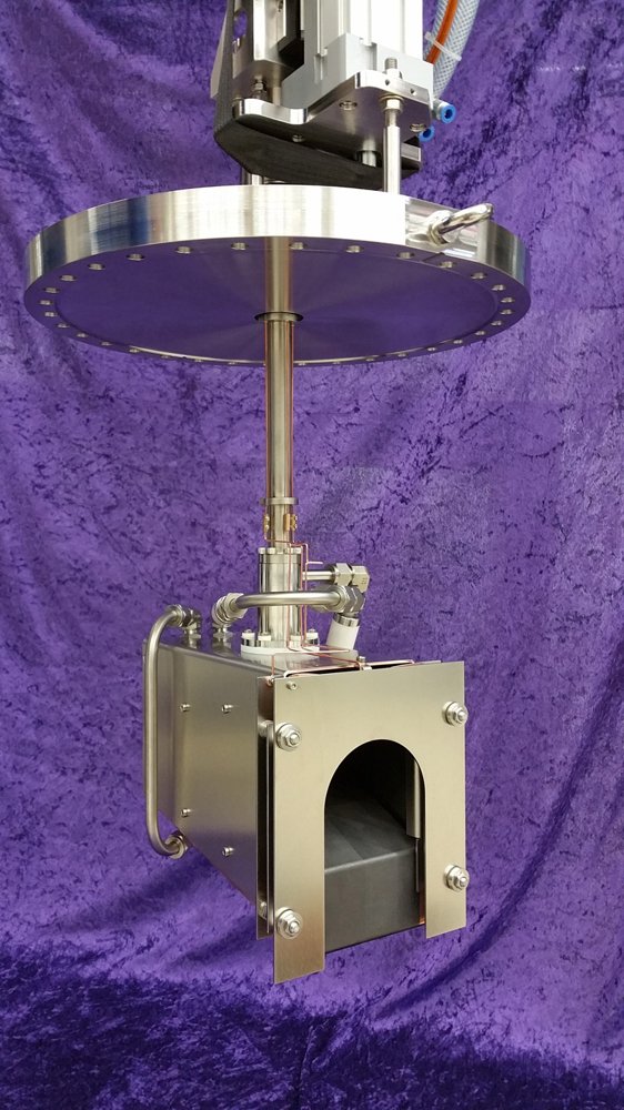
The principle of operation is rather simple: the ion beam is hitting a piece of metal, the current flow to earth is measured with an ammeter and corresponds to the beam current. For practical implementation, however, there are a number of edge effects to consider: 1. Secondary electron suppression. Secondary electrons are leaving the surface when the beam comes in. They make a positive contribution to the measured total current and thus distort the result. A aperture at negative potential pushes the electrons back again and thus suppresses this effect. 2. The beam power must be dissipated thermally. With intense ion beams, critical values of a few kW per square centimeter are easily reached. Cooling with water is required. 3. In the time-resolved high-resolution measurement from about 1MHz a so-called fast Faraday cup is needed. This corresponds to a 50 ohm geometry. The termination (internal resistance of the ammeter) must be correspondingly low-ohmic to keep the time constant low. 4. If there is a risk of activation, materials with a low atomic number can become interesting. As an example, we also offer cups in graphite finish, also prepared with a water cooling system for high power applications. The applications are very different, like our solutions. Please confront us with your specific wishes, name us your characteristic parameters such as the expected beam current, the particle species, the beam energy, the beam spot size and the required aperture, movable to linear drive or stationary. We will certainly find an optimized solution.
CATEGORY
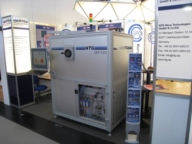
The Ion Beam Figuring Plant – IBF 100 – is a procedural plant for nanometer exact correction of small surfaces. The IBF 100 is a consistent advancement of our bigger plants IBF 300,IBF 450 and IBF 700. The last mentioned plants are sold with great success for nearly 25 years. They are used in the high-end-processing of predominantly large shaped optical parts (PV-value <λ/100, λ=633nm – rms-values <1nm – lenses for stepper objectives in the semiconductor production). However, the IBF 100 has been developed to optimize surfaces of small shaped parts within shortest time from PV values in the range of λ/5 as input parameter to λ/10 and better. Special attention has turned to short length of cycles. Parts with a diameter of 5-70mm, a max. part thickness of 45mm and a max. angle of 60° can be treated. The components can be onvex, plane or concave. In principle there are nearly any restrictions for the treatment of geometries within the afore mentioned dimensions. TECHNICAL DATA Plant, complete Dimensions: length: 1560mm width: 1300mm height: 2170mm, incl. superstructural parts required space Area: diameter 4m or 3x3m weight: 1.850kg Workpiece data - max. diameter: 70mm - max. thickness: 45mm incl. support, respectively holder - max. contact angle: 60°
CATEGORY
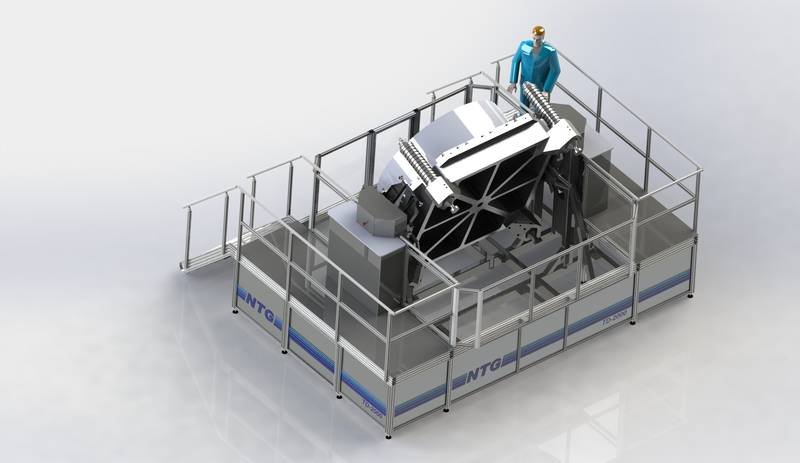
The Turning Device 2000 is a device for assembling, fine adjusting and turning optical components up to a diameter of 2000mm. The device is optimized for the use with an IBF 2000. The original workpiece holder of the IBF 2000 can be adapted to the TD 2000 by using a lifting device (crane, etc.). The device is independent from the IBF plant, so it is possible to prepare a second substrate for IBF treatment while a first one is processed. The TD 2000 is a semi-automatic, motor driven device. In case of any power loss the device stops at the current position. Safety precautions are implemented according to the actual state of the art and regulations. The platform including two stairs enables easy, safe and convenient handling. The operation is controlled via several push buttons located on the operating panel on the left platform side. The footprint of the device is 4.7m(depth) by 5.3m(width), the maximum required height (workpiece in vertical orientation) is 3.8m.
CATEGORY
