By Comet Yxlon
Streamlined, seamless communication between systems, software and people is critical for the efficiency and productivity of the overall inspection process. The Comet Yxlon Software Suite supplies you with a range of powerful connectivity packages, including automation features for recurring inspection tasks, hassle-free image data transfer between systems and facilities, or automated X-ray dose tracking. A selection of our Efficiency Software packages & features: - Batch Manager - Dose Manager - Automatic Data Transfer - ProLoop and more!
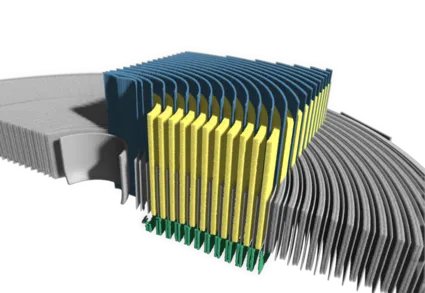
From effortless visualization to AI-based segmentation and quantification – Dragonfly 3D World delivers the features you need for quick and meaningful results. Powerful CT requires powerful visualization. Dragonfly, now available with Comet Yxlon Equipped with an advanced machine learning based segmentation engine, the Dragonfly 3D World user-friendly interface enables scientists and engineers to extract powerful qualitative and quantitative findings from images with ease. Get quantitative answers for your most demanding 2D, 3D, and 4D imaging studies – including data from correlative and hyperspectral imaging systems, X-ray, SEM, FIB-SEM, confocal microscopy, and many more! Dragonfly 3D World Highlights: - Easy-to-use, intuitive, and customizable interface - Import of 2D/3D/4D images, volumetric data, and proprietary data types from multiple sources - Post-processing functions for data restructuring, filtering, volume and slice registration, image stitching etc. - Deep-learning based image enhancement and segmentation - Automation of 3D analysis workflows with macros Using Dragonfly deep learning for efficient and reliable segmentation AI solutions developed with state of the art deep learning models offer numerous benefits for segmentation and CT image analysis in science and research. By accurately and efficiently identifying patterns, objects, and anomalies in large volumes of images, researchers can save time and effort. Additionally, the smart technology helps improve the reproducibility and reliability of image analysis by reducing operator bias – with significant potential for advancing scientific research in fields such as biology, materials science, and additive manufacturing. Dragonfly helps you unlock the power of deep learning and extract more value from your images. It offers a wide set of tools for any image analysis requirement and allows you to adapt and refine your own DL models with wizard-based training. Quality Assurance Industrial inspection of electronics, castings, plastic injection and additive manufacturing parts. Non-destructive testing (NDT) with X-ray computed tomography helps manufacturers monitor and optimize both their product and process quality. With Dragonfly 3D World, industrial users can unleash the true potential of scientific image processing for their inspections – and gain unique insights into the critical areas of parts and components. Quantitative analysis: count, measure, deliver. Whether you are analyzing pores, fibers, grains or phases, Dragonfly 3D World’s quantification and analysis tools give you powerful options for counting, measuring, and characterizing image features. Porosity and void analysis: Dragonfly 3D World's automated thresholding tools enable fast and efficient segmentation of casting or electronics parts. Porosity and voids can be calculated, visualized, and analyzed by size or volume using color coding, allowing for detailed examination of internal structures and defect identification. Wall thickness analysis: Create detailed renderings that highlight varying thicknesses and their distribution within inspection parts. Use color-coding to differentiate thickness levels or provide comprehensive statistical analyses for deeper insights. Size, shape, and spatial properties: Make measurements on hundreds to millions of individual grains, pores, organelles, etc. Select from volume, surface area, Ferret diameter, aspect ratio, roughness, sphericity and scores of additional measurements. Analyze and classify - Cross-index measurements between analyses or across samples to answer nuanced research questions - Plot histograms to gain insights into the distribution and characteristics of your data and categorize objects according to specific criteria - Map out layer thicknesses and probe depth maps to understand biases in spatial distributions - Identify and evaluate three-phase boundaries and interfacial surface areas Meshes and models: Produce high-quality meshes, vector fields, and spatial graphs from image data, segmentations, or simulations. These elements are generated with precision to meet complex scientific and industrial needs. Numerical modeling options - Color-coded scalar meshes of local thickness, curvature, and deviation maps - Perform a wide range of pore network simulations with OpenPNM - Perform material response simulations on the microstructures of porous media with PuMA - Quantify fluid flow and heat dissipation with NGSolve - Investigate the inter-relationship between connected components Deviation from design: Does the final manufactured part conform to its original design? By importing the design mesh file (STL) Dragonfly 3D World allows the comparison of this file with the actual part. Color coding can be used to highlight the largest deviations or warping. Fiber analysis: Calculating the physical properties of composites, polymers, and fibrous materials with Dragonfly 3D World provides researchers and product developers with the comprehensive understanding of material behavior that is essential for improving and developing new products. More applications - Automated extraction of individual fibers from reinforced composites - Computation of microstructural characteristics, such as fiber length and tortuosity, orientation, thickness - Examination of the interface between fibers and matrix material in composites
CATEGORY
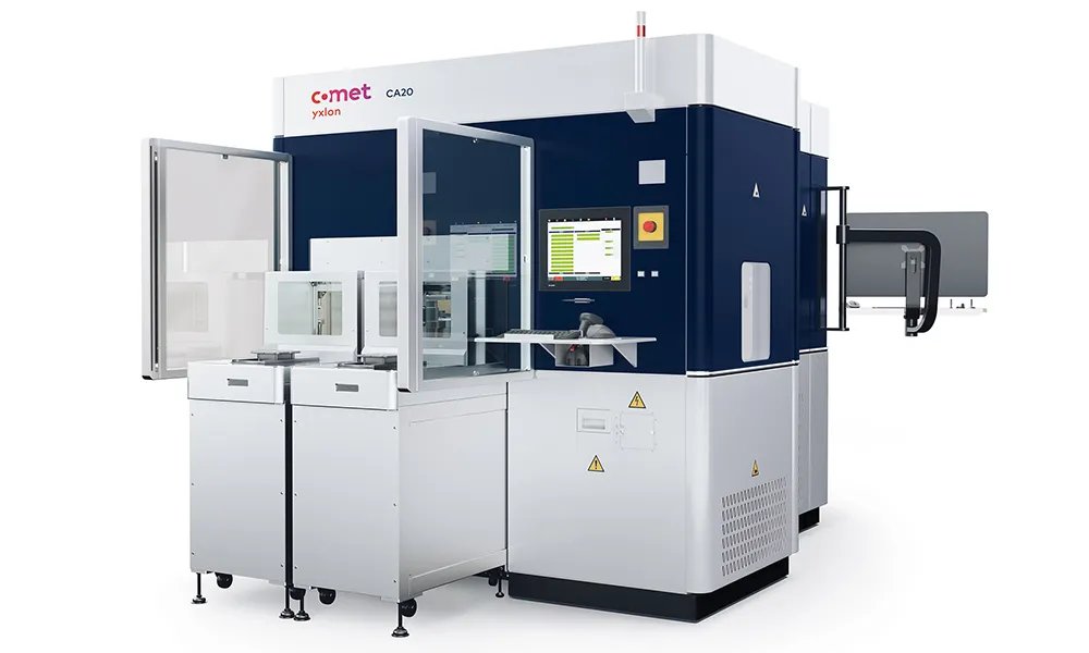
Designed to cover the entire semiconductor manufacturing chain, from wafer processing to packaged chip s Available with fully automated operation for seamless integration into your fab AI-based data analysis and advanced software ensures fast, accurate defect classification to resolve systematic issues and maximize yield Non-destructive technology for three-dimensional insights into solder bumps or TSVs within minutes Repeatable results through reliable and accurate technology, designed to support a stable inspection routine Cleanroom ready, with conditions within the cabinet comparable to ISO Class 3 With thousands or millions of tightly packed, nearly identical TSVs on a single wafer, accurately segmenting and positioning these elements poses a significant challenge even for modern inspection techniques. The CA20 optimises for speed and accuracy with a 2.5D approach, capturing 2D images at various angles to retain depth information. This aids in determining positioning, requires less contrast for the visualisation of critical voids, reduces scan time, and provides a statistically relevant overview of the entire wafer. Especially when combined with our AI-powered software packages like TSV Insights X 2.5D, CA20 can now help you find critical semiconductor defects fast across the entire manufacturing chain. By combining high-resolution 3D and 2.5D X-ray capabilities with AI-driven automatic defect classification (ADC), the CA20 helps to detect systematic challenges faster than ever before. Available as a fully-automated solution, it seamlessly integrates into the Fab’s material and information flows to deliver actionable real-time metrology data for assuring product quality and maximizing yield. While inspections using destructive methods can take weeks, 3D X-ray gives your R&D engineers results they can work with right away. As a non-destructive testing (NDT) system, the CA20 supplies you with crystal-clear 3-dimensional images of nano details inside your ICs within minutes. Monitor your interconnects process, find flaws fast and feed your insights back into the process. 3D X-ray produces high-resolution 3D volumes that allow manufacturers to measure and inspect bumps and identify smallest defects in record time. See critical defects such as non-wet, head-in-pillow or bump shift and determine the stand-off height to monitor die tilt or warping like never before. Whether you need the highest quality images to inspect your parts in a Lab/R&D environment, or you require a fully-automated solution that easily fits into your existing production process, the CA20 is available in a variety of configurations to suit your needs. Small batch inspection & failure analysis. While inspections using destructive methods can take weeks, 3D X-ray gives your R&D engineers results they can work with right away. Quickly ramp-up your interconnects process and find flaws fast with feedback gained from 3D images within minutes. Fully-automated inspection. Our smart 3D X-ray inspection solution - for the fab. With a fully automatic loader and ADC software, the CA20 is designed to complement your production line with consistent, fast and accurate 3D X-ray inspection. Monitor your interconnects process, recognize flaws fast and feed your insights back into the process. CA20 inspection applications in R&D and production - Chip-on-Substrate including Fan Out packaging solder connections (C4 bumps and copper pillars) - 2.5 and 3D IC package solder connections including microbumps - TSV inspection - Substrate strip solder bumps - Sensors - MEMS and MOEMS Technical Data Application/Version MXI / Lab AXI / Fab Max. inspection envelope 435 mm (17")435 mm (17") System Dimensions (W/D/H)1650 x 1400 x 2050 mm 1955 x 3100 x 2200 mm System Weight~2350 kg~ 3650 kg Detector Active Area 130 x 130 mm 130 x 130 mm Pixel Matrix 1536 x 1536 px 1536 x 1536 px Pixel Pitch 85 µm 85 µm Oblique Viewing+/- 65° (130°)+/- 65° (130°) Max. part weight 1 - 2 kg 0.5 kg Scan Modes 2D, 2.5D, 3D 2D, 2.5D, 3D Depending on fan filter unit / cleanroom class. Max. part weight: 1 kg (on carbon plate), 2 kg (on part holder if fixed on the table side). Accumulated weight of all parts incl. weight of carrier
CATEGORY
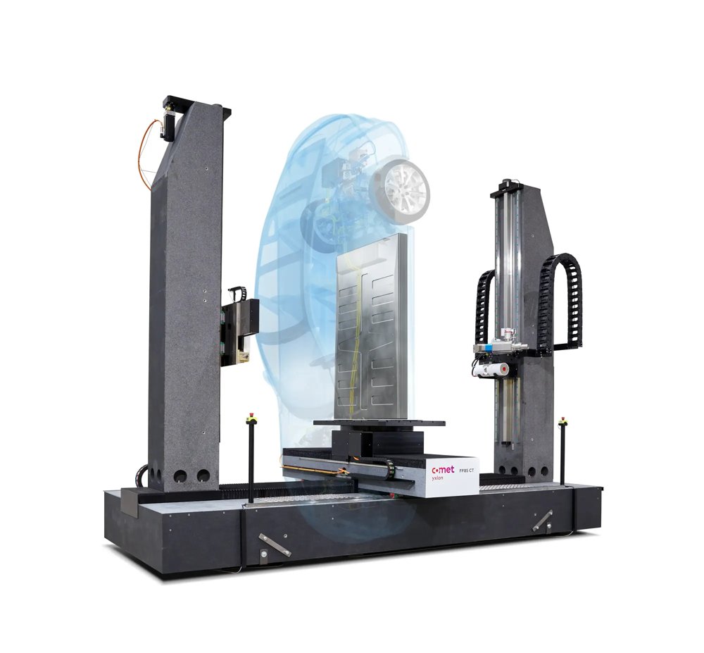
FF85 CT highlights: - Extensive range of applications from microCT to high-energy CT due to dual tube configuration and both flat-panel and line detector - Large inspection envelope by diverse field-of-view extensions, helical and dual-helical CT techniques - Granite base for temperature stability and precise manipulation - Maximum versatility through up to 7 manipulation axes - Intuitive Geminy user interface with touchscreens for easy system operation - Available in several configurations, including handling parts of unprecedented size—up to 1000 kg! - NEW!The 225 kV X-ray tube is now available with a High Density Power (HDP) Target. More power density, faster inspection and improved resolution High energy. High resolution. High versatility. Small parts or large parts, the optional combination of two X-ray tubes with a spacious flat-panel detector (DDA – digital detector array) and a linear detector array (LDA) caters to the broadest application range. While the mini-focus tube, with its high energy of up to 600 kV, is the right solution for large and dense parts, the directional micro-focus tube (up to 300 kV) provides detailed insights into the inner structures of small components. Seamless switches between 2D radioscopy, 3D cone-beam, and fan-beam CT provide outstanding flexibility and the creation of individual inspection processes. Almost indestructible: the granite-based manipulator Another building block that contributes to the premium performance of FF85 CT is the rock-solid granite-based manipulator. It makes the system extremely precise and durable by providing warp resistance and temperature stability. Various trajectories for maximum flexibility Graphic symbols and a wide range of automated functions, displayed on the intuitive user interface Geminy make operation easy – regardless of the operator’s skill level. At the same time, it offers a great number of features for flexibility regarding part sizes and inspection tasks, like CT trajectories such as HeliExtend (helical CT scan and reconstruction method), horizontal and vertical field-of-view extensions, a virtual rotation axis, and standard quick/quality scans. Image enhancement tools like ScatterFix 2.0, beam hardening reduction (BHC), or metal artifact reduction (MAR) reduce or eliminate scattered radiation or artifacts in the image. Think big. The latest configuration of the proven FF85 CT offers a new dimension of scanning possibilities for the automotive and other industries. The CT system allows the nondestructive inspection of largest parts, such as complete EV battery packs, in ultra-short time and unmatched resolution. With its unique variety of CT trajectories, the large-sized FF85 CT is the flexible expert for a wide range of scanning tasks from micro to macro – and a future-proof investment enabling a fast ROI. The full technical specifications can be found in the flyer within the downloads section below. Which items can be inspected with the FF85 CT? - Aluminum, steel, and super alloy components - Additively manufactured parts - Battery cells, modules, and systems - Fiber-reinforced composites - Plastic injection molded parts - Cultural assets, historical art, and archeological objects - Geological, paleontological and biological samples - Mechatronic modules Which applications is the FF85 CT designed for? - Material and structural analysis in research and development - First article inspection - Dimensional measurement - Small series inspection - Failure analysis - Assembly checks - Digitization - Segmentation Technical Data Sample Diameter (1)up to 1800 (mm) Sample Height (1)up to 3000 [mm] Maximum Sample Weight (1)1000 [kg] Focus-Detector-Distance (FDD) (2)up to 3700 [mm] Available X-ray Tubes 600 kV Minifocus, 450 kV Minifocus, 450 kV Mesofocus, 300 kV Microfocus, 225 kV Microfocus, 190 kV Nanofocus Available X-ray Detector Flat-panel detector, Line detector array Available CT Modes Cone-beam CT, QuickScan, QualityScan, HeliExtend, FlexCenter (virtual rotation axis), ZoomScan, LayerScan, SpeedMode, Fan-beam CT, ScanExtend (FoV extensions), Volume crop Manipulation 7 axes, granite base (1) Depends on configuration chosen. This figure shows the configuration for extra-large parts (2) Specification shown for minifocus & line detector
CATEGORY
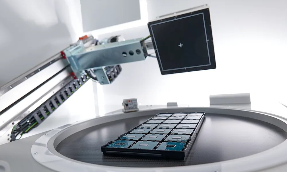
Cheetah EVO highlights - Fast and intuitive scan set-up - High detail resolution at submicron level for 2D, 2.5 D and 3D imaging - Best-in-class laminography - Automated inspection programs and software-assisted image review - Dose monitoring for sensitive parts - Optional high load capacity (≤20 kg) - Seamlessly integrated 3D visualization with optional AI-powered image analysis The Cheetah EVO responds to the need for improved, automated operation with integrated workflows in the FGUI operating software. 3D volumes once acquired and reconstructed are brilliantly visualized using Dragonfly 3D View. They can be analyzed with Dragonfly 3D World, which takes advantage of an AI-powered image processing algorithm. Both Dragonfly software solutions offer the ability to render 3D cinematic images with a preset selection using application-specific look-up tables resulting in the most realistic, vivid visualization. In today’s smart factory, everything revolves around connectivity and self-optimizing processes. Industry 4.0 demands for quality control systems that offer improved automated inspections and can become an integral part of the production line. Based on customer input, Comet Yxlon upgraded the Cheetah EVO system with advanced features that help manufacturers reach new heights in speed, image quality, reliability, and repeatability. SMT inspections: grand performance for small devices Due to the continuous miniaturization of electronic components, more and more features must fit in an ever-smaller area. For the most accurate and repeatable quality inspection results, a test system must not only provide high performance and resolution but also needs to be equipped with dynamic image enhancement filters. The Comet Yxlon Cheetah EVO features: Large flat-panel detectors with up to 50% larger field of view for a better overview and faster working processes due to reduced steps in automated processes Best laminography with micro3Dslice, with detailed 3D visualization for quick and easy failure analysis – resulting in substantial cost-savings compared to micro sectioning Automatic void calculation with VoidInspect CL or DR, the laminography- or radiscopy-based inspection workflows enabling the rapid non-destructive analysis of voids inside the solder joints of board components ProInspect THTInspect DR, the semi-automated defect analysis for fill level inspections on THT-based components in 2D Optional high load capacity (< 20 kg) with reinforced table and mechanics: Several parts and electronic interconnects in fixed packages can be inspected at once – a real-time saver Cheetah EVO SMT applications - PCB (BTC, BGA, LGA, QFN/QFP, THT) - IGBT - LED Semicon inspections: maximum resolution at minimum voltage Electronic components and semiconductor devices are the key elements of most electronic systems. Due to their compactness and density, testing requires maximal image resolution at low power and low voltage. Void compilations, including multi-area voiding, need accurate, repeatable inspection routines. The Comet Yxlon Cheetah EVO offers: - Highly sensitive detector with optional low dosage mode - High detail recognition through an integrated image chain - Integrated, automatic defect detection with FGUI (e.g. voids in bumps) Cheetah EVO semiconductor applications - Wafers and integrated circuits (IC): Die attach connections, 3D IC joints, TSV - Sensors - MEMS and MOEMS Laboratory inspections: leading technology for precise analysis The inspection of electronic components during research and development is highly complex and requires a broad range of features. Computed tomography with the Comet Yxlon Cheetah EVO is the technology of choice for detailed analyses of micro components such as those used in batteries, connectors, and medical devices. Exceptional CT quality due to a range of highly sensitive detectors with excellent contrast-to-noise ratio Realistic, vivid visualization by Comet Yxlon FF CT software, integrated with the FGUI user interface workflows with individual 3D cinematic renderers, artifact reduction, and a preset selection of transfer functions (TF) Cheetah EVO lab applications - Batteries - Connectors - Various hard-to-see electronics components - Medical material - Military and space electronics Technical Data Sample Size 800 x 500 [mm] (31'' x 19'') Max. Radioscopic Area 460 x 410 [mm] (18'' x 16'') System Dimensions (W/D/H)1650 x 1400 x 2050 [mm] System Weight 2200 kg FeinFocus X-ray Tube FXT-160.50 Microfocus or FXT-160.51 Multifocus, 20 - 160 kV voltage range Pixel Matrix 1004 x 620 px (Flat-panel detector 1308), 1004 x 1004 px (Flat-panel detector 1313), 1276 x 1276 px (Flat-panel detector 1616) Pixel Pitch 127 µm Bit Depth 16 bit Oblique Viewing+/- 70° (140°) 3D Modes Laminography (micro3Dslice), CT QuickScan, QualityScan
CATEGORY
