By MEMSIC Inc.
FEATURES Better than 1 mg resolution Dual axis accelerometer fabricated on a monolithic CMOS IC RoHS compliant On-chip mixed mode signal processing No moving parts 50,000 g shock survival rating 17 Hz bandwidth 3V to 5.25V single supply continuous operation Small (5.5mm x 5.5mm x 2.7mm) LCC XY/YZ sensing package Continuous self test APPLICATIONS Automotive – Vehicle Security/Active Suspension/ABS Headlight Angle Control/Tilt Sensing Security – Gas Line/Elevator/Fatigue Sensing Office Equipment – Computer Peripherals/PDA’s/ Cell Phones Internal Oscillator White Goods – Spin/Vibration Control GENERAL DESCRIPTION The MXR2500MW is an ultra low noise and low cost, dual axis accelerometer fabricated on a standard, submicron CMOS process. It is a complete sensing system with on-chip mixed mode signal processing. The MXR2500MW measures acceleration with a full-scale range of 2 g and a sensitivity of 500mV/g @5V at 25 C. It can measure both dynamic acceleration (e.g., vibration) and static acceleration (e.g., gravity). The MXR2500MW design is based on heat convection and requires no solid proof mass. This eliminates stiction and particle problems associated with competitive devices and provides shock survival of 50,000 g, leading to significantly lower failure rates and lower loss due to handling during assembly. The MXR2500MW provides two absolute analog outputs. The typical noise floor is 0.2 m g/Hz allowing signals below 1 m g to be resolved at 1 Hz bandwidth. The 3dB rolloff of the device occurs at 17 Hz. The MXR2500MW is available in a LCC surface mount package (5.5 mm x 5.5 mm x 2.7 mm). It is hermetically sealed and is operational over a -40 C to +105 C temperature range. It also contains an on-chip temperature sensor and a bandgap voltage reference. MXR2500MW SPECIFICATIONS (Measurements @ 25 C, Acceleration = 0 g unless otherwise noted; V DD, V DA =5.0V unless otherwise specified) Parameter Conditions Min MXR2500MW Typ Max Units SENSOR INPUT Measurement Range 1 Each Axis 2 g Nonlinearity Best fit straight line 0.5 1.0 % of FS Alignment Error 2 1.0 degree Transverse Sensitivity 3 2.0 % SENSITIVITY Sensitivity, Analog Outputs at pins AOUTX and A OUTY 4 Each Axis 475 500 525 mV/ g Change over Temperature from 25 C -25 +8 % ZERO g BIAS LEVEL 0 g Offset 4 Each Axis -0.1 0.00 +0.1 g 0 g Voltage 4 2.50 V 0 g Offset over Temperature from 25 C from 25 C, based on 500mV/ g 1.5 0.75 mg/C mV/ C NOISE PERFORMANCE Noise, rms 0.2 0.4 mg/Hz FREQUENCY RESPONSE 3dB Bandwidth - uncompensated 17 Hz TEMPERATURE OUTPUT Tout Voltage 1.15 1.25 1.35 V Sensitivity 4.6 5.0 5.4 mV/ C VOLTAGE REFERENCE OUTPUT VRef output @3V-5.25V supply 2.5 V Change over Temperature 0.1 mV/ C Current Drive Capability Source 100 A SELF TEST Continuous Voltage at A OUTX, A OUTY under Failure supply voltage 5.0 V AOUTX and A OUTY OUTPUTS Normal Output Range 1.0 4.0 V Current Source or sink, @ 3.0V-5.25V supply 100 A Turn-On Time 5 160 mS POWER SUPPLY Operating Voltage Range 3.0 5.25 V Supply Current 3.5 mA TEMPERATURE RANGE Operating Range -40 +105 C NOTES 1 Guaranteed by measurement of initial offset and sensitivity. 2 Alignment error is specified as the angle between the true and indicated axis of sensitivity. 3 Transverse sensitivity is the algebraic sum of the alignment and the inherent sensitivity errors. 4 The device operates over a 3.0V to 5.25V supply range. Please note that sensitivity and zero g bias level will be slightly different at 3.0V operation. For devices to be operated at 3.0V in production, they can be trimmed at the factory specifically for this lower supply voltage operation, in which case the sensitivity and zero g bias level specifications on this page will be met. Please contact the factory for specially trimmed devices for low supply voltage operation. 5Output settled to within 17mg. ABSOLUTE MAXIMUM RATINGS* Supply Voltage (V DD, V DA ) ………………...-0.5 to +7.0V Storage Temperature ……….…………-65 C to +150 C Acceleration ……………………………………..50,000 g *Stresses above those listed under Absolute Maximum Ratings may cause permanent damage to the device. This is a stress rating only; the functional operation of the device at these or any other conditions above those indicated in the operational sections of this specification is not implied. Exposure to absolute maximum rating conditions for extended periods may affect device reliability. PACKAGE CHARACTERISTICS Package JA JC Device Weight LCC-8 110 C/W 22 C/W < 1 gram PIN DESCRIPTION: LCC-8 PACKAGE Pin Name Description I/O 1 TOUT Temperature (Analog Voltage) O 2 Gnd Ground I 3 VDA Analog Supply Voltage I 4 AOUTX X-Axis Acceleration Signal O 5/J VDD Digital Supply Voltage I 6/M Vref 2.5V Reference Output O 7/L Sck Optional External Clock I 8/K AOUTY Y-Axis Acceleration Signal O ORDERING GUIDE Model Package Style MXR2500MW LCC8 RoHS compliant *LCC parts are shipped in tape and reel packaging. CAUTION ESD (electrostatic discharge) sensitive device. THEORY OF OPERATION The MEMSIC device is a complete dual-axis acceleration measurement system fabricated on a monolithic CMOS IC process. The device operation is based on heat transfer by natural convection and operates like other accelerometers having a proof mass except it is a gas in the MEMSIC sensor. A single heat source, centered in the silicon chip is suspended across a cavity. Equally spaced aluminum/polysilicon thermopiles (groups of thermocouples) are located equidistantly on all four sides of the heat source (dual axis). Under zero acceleration, a temperature gradient is symmetrical about the heat source, so that the temperature is the same at all four thermopiles, causing them to output the same voltage. Acceleration in any direction will disturb the temperature profile, due to free convection heat transfer, causing it to be asymmetrical. The temperature, and hence voltage output of the four thermopiles will then be different. The differential voltage at the thermopile outputs is directly proportional to the acceleration. There are two identical acceleration signal paths on the accelerometer, one to measure acceleration in the x-axis and one to measure acceleration in the y-axis. PIN DESCRIPTIONS TOUT – This pin is the buffered output of the temperature sensor. The analog voltage at T OUT is an indication of the die temperature. This voltage is useful as a differential measurement of temperature from ambient and not as an absolute measurement of temperature. After correlating the voltage at TOUT to 25 C ambient, the change in this voltage due to changes in the ambient temperature can be used to compensate for the change over temperature of the accelerometer offset and sensitivity. Gnd – This is the ground pin for the accelerometer. VDD – This is the supply input for the digital circuits and the sensor heater in the accelerometer. The DC voltage should be between 3.0 volts and 5.25 volts. VDA – This is the power supply input for the analog amplifiers in the accelerometer. AOUTX – This pin is the output of the x-axis acceleration sensor. The user should ensure the load impedance is sufficiently high as to not source/sink >100 A. While the sensitivity of this axis has been programmed at the factory to be the same as the sensitivity for the y-axis, the accelerometer can be programmed for non-equal sensitivities on the x- and y-axes. Contact the factory for additional information on this feature. AOUTY – This pin is the output of the y-axis acceleration sensor. The user should ensure the load impedance is sufficiently high as to not source/sink >100 A. While the sensitivity of this axis has been programmed at the factory to be the same as the sensitivity for the x-axis. Sck – The standard product is delivered with an internal clock option (800kHz). This pin should be grounded when operating with the internal clock. Vref – This pin is the output of a reference voltage. It is set at 2.50V typical and has 100 A of drive capability. RESOLUTION The accelerometer resolution is limited by noise. The output noise will vary with the measurement bandwidth. With the reduction of the bandwidth, by applying an external low pass filter, the output noise drops. Reduction of bandwidth will improve the signal to noise ratio and the resolution. The output noise scales directly with the square root of the measurement bandwidth. The maximum amplitude of the noise, its peak- to- peak value, approximately defines the worst case resolution of the measurement. With a simple RC low pass filter, the rms noise is calculated as follows: Noise (mg rms) = Noise(mg/ Hz ) )6.1 )(( Hz Bandwidth The peak-to-peak noise is approximately equal to 6.6 times the rms value (for an average uncertainty of 0.1%). EXTERNAL FILTERS AC Coupling: For applications where only dynamic accelerations (vibration) are to be measured, it is recommended to ac couple the accelerometer output as shown in Figure 4. The advantage of ac coupling is that variations from part to part of zero g offset and zero g offset versus temperature can be eliminated. Figure 4 is a HPF (high pass filter) with a –3dB breakpoint given by the equation: RC f 21. In many applications it may be desirable to have the HPF –3dB point at a very low frequency in order to detect very low frequency accelerations. Sometimes the implementation of this HPF may result in unreasonably large capacitors, and the designer must turn to digital implementations of HPFs where very low frequency –3dB breakpoints can be achieved. Low Pass Filter: An external low pass filter is useful in low frequency applications such as tilt or inclination. The low pass filter limits the noise floor and improves the resolution of the accelerometer. The low pass filter shown in Figure 5 has a –3dB breakpoint given by the equation: RC f 21. For the 200 Hz ratiometric output device filter, C=0.1 F and R=8k, 5%, 1/8W. TEMPERATURE OUTPUT NOISE REDUCTION It is recommended that a simple RC low pass filter is used when measuring the temperature output. Temperature output is typically a very slow changing signal, so a very low frequency filter eliminates erroneous readings that may result from the presence of higher frequency noise. POWER SUPPLY NOISE REJECTION Two capacitors and a resistor are recommended for best rejection of power supply noise. The capacitors should be located as close as possible to the device supply pins (V DA, V DD ). The capacitor lead length should be as short as possible, and surface mount capacitors are preferred. For typical applications, capacitors C1 and C2 can be ceramic 0.1 μF, and the resistor R can be 10 Ω. PCB LAYOUT AND FABRICATION SUGGESTIONS 1. The Sck pin should be grounded to minimize noise. 2. Liberal use of ceramic bypass capacitors is recommended. 3. Robust low inductance ground wiring should be used. 4. Care should be taken to ensure there is “thermal symmetry” on the PCB immediately surrounding the MEMSIC device and that there is no significant heat source nearby. SOLDER REFLOW PROFILE 1. Reflow is limited by 2 times. Second reflow should be applied after device has cooled down to room temperature (25℃). 2. Recommended reflow profile for Pb free process is shown in below figure. The time duration of peak temperature (260℃) should be limited to 10 seconds. STENCIL DESIGN 1. It is recommended to use a stencil of thickness between 0.12mm~0.18mm. Stencil thickness should consider all devices on the PCB. It is suggested to select relatively thicker stencil to ensure adequate solder volume. 2. Stencil opening ratio is suggested between 0.8~1.4. 1:1 is a regular opening ratio. To increase the solder volume, a larger opening ratio is recommended. END of LIFE DISPOSAL End-of-life products should be disposed/ recycled properly in accordance to national and local regulation. LCC-8 PACKAGE DRAWING CERAMIC (BLACK) Dimensions show in (mm) Tolerance: ±0.2 (Unless otherwise specified)
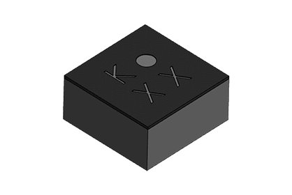
WLP package, 0.85x0.85x0.4mm, I²C/I³C interface, ±30g range, high performance AMR Magnetometer Application: Smart Phone/Pad/NoteBook; Wearable Device; Smart Home; Smart Device Monolithic integrated 3-axis AMR magnetic sensor and electronic circuits requiring fewer external components Superior Dynamic Range and Accuracy ±30 G FSR 20bits operation mode 0.0625mG per LSB resolutio 2 mG total RMS noise Enables heading accuracy of ±1º Sensor true frequency response up to 1KHz Ultra-Small Wafer Level Package 0.8x0.8x0.4mm On-chip automatic degaussing with built-in SET/RESET function Eliminates thermal variation induced offset error (Null field output) Clears the residual magnetization resulting from strong external fields On-chip sensitivity compensation On-chip temperature sensor Selftest signal available Dataready Interrupt (I³C only) Low power consumption 1µA power down current I²C slave, FAST (≤400 KHz) mode I³C interface, Compatible with MIPI I³C pecfication version 1.0 1.62V to 3.6V wide range single power supply 1.2V compatible I²C interface 1.8V 1.8V compatible I³C interface RoHS complian
CATEGORY
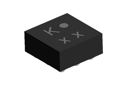
BGA package, 1.2x1.2x0.5mm, I²C interface, ±30g range, high performance AMR Magnetometer Application: Wearable Device, Smart Home, Smart Device Fully integrated 3-axis magnetic sensor and electronic circuits requiring fewer external components Superior Dynamic Range and Accuracy ±30G FSR with 16bits operation 1mG per LSB resolution 2mG total RMS noise Enables heading accuracy of 1º Output data rate up to 600 Hz Ultra Small Low profile package 1.2x1.2x0.5mm Degaussing with built-in SET/RESET function Eliminates thermal variation induced offset error (Null field output) Clears the residual magnetization resulting from strong external fields On-chip sensitivity compensation On-chip temperature sensor MotionDetection and DataReady Interrupt Low power consumption 1µA power down current I²C Slave, FAST (≤400 KHz) mode 1.8V single low power supply compatible Low to 1.2V I²C interface RoHS compliant
CATEGORY
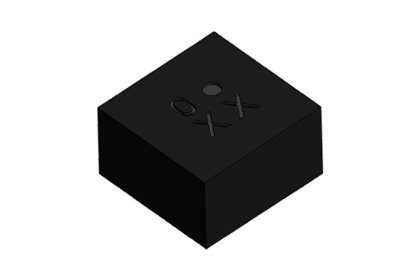
BGA package, 1.6x1.6x0.6mm, multiple I²C device addresses, I²C interface, ±16g range, high performance AMR Magnetometer Fully integrated 3-axis magnetic sensor and electronic circuits requiring fewer external components Superior Dynamic Range and Accuracy ±16G FSR with 16/14bits operation 0.5mG/2mG per LSB resolution in 16/14bits operation mode 1.5mG total RMS noise Enables heading accuracy of ±1º Max output data rate of 800 Hz (12 bits mode) Ultra Small Low profile package 1.6x1.6x0.6mm Allows for elimination of temperature variation induced offset error (Null field output) Clears the sensors of residual magnetization resulting from strong external fields On-chip sensitivity compensation Low power consumption (140µA @ 7Hz ) 1µA (max) power down function I²C Slave, FAST (≤400 KHz) mode 1.62~3.6V wide power supply operation supported, 1.8 V I/O compatibility RoHS compliant
CATEGORY
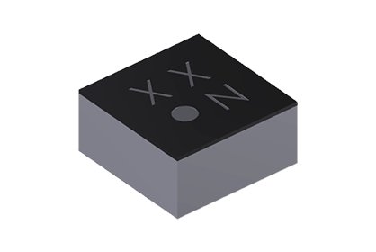
WLP package, 0.8x0.8x0.4mm, I²C interface, ±30g range, high performance AMR Magnetometer Monolithic integrated 3-axis AMR magnetic sensor and electronic circuits requiring fewer external components Superior Dynamic Range and Accuracy ±30G FSR 20bits operation mode 0.0625mG per LSB resolution 2mG total RMS noise Enables heading accuracy of 1º Sensor true frequency response up to 1KHz Ultra-Small Wafer Level Package 0.8x0.8x0.4mm On-chip automatic degaussing with built-in SET/RESET function Eliminates thermal variation induced offset error (Null field output) Clears the residual magnetization resulting from strong external fields On-chip sensitivity compensation On-chip temperature sensor Selftest signal available Low power consumption 1µA power down current I²C slave, FAST (≤400 KHz) mode 1.62V to 3.6V wide range single power supply 1.2V logic IO RoHS compliant
CATEGORY
