By SELA
Adaptive Ion Milling utilized in Xact200 system provides sufficient solution for delayering and cross-section of V-NAND structures in delivering wide
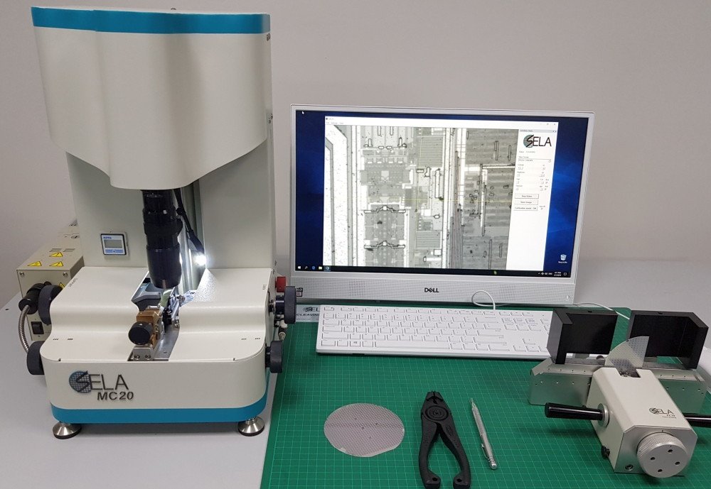
The SELA MC20 smart micro cleaving system with capability to register and cleave buried defects is the advanced solution for the SEM sample preparation of crystalline materials with high quality, high accuracy and high throughput. The MC20 utilizes and delivers to customers enhanced capabilities of wining SELA’s Micro Cleaving technology together with the state-of-the-art optics. The MC20 smart table top system, equipped with masterly designed comprehensive optical solution combined regular white and special IR optics, achieves semi-automatic, reliable, repeatable and rapid cross-sectioning of wafer segments and dies with high cleaving accuracy. Observation from top and back sides of the sample provides strong additional capability for the failure analysis of buried defects. This capability answers to challenges in analysis of all kinds of failures in semiconductors, MEMS devices, dies extracted from package and others. Dedicated software enables the accurate positioning control and alignment of the cleaving elements. Cleaved samples are ready for immediate inspection and analysis. The set of the MC20 together with PCM and TMO features target marking, extraction of the initial sample and final cross-sectioning with high throughput, high consistent accuracy and the excellent natural lattice quality of the cross-sections produced. Such advanced capabilities of the set of the MC20 significantly reduce the turnaround time for failure analysis and process monitoring. ENHANCED CAPABILITIES - Semi-automatic controllable cleaving process for visible and buried defects - Observation from top and bottom sides of the sample - Registration and cross-section of buried defects - Advanced white light and IR optics FEATURES - Accuracy better than 5 microns, mostly 2-3 microns - Process time – single minute - Small input sample or die – down to 4×2 mm - Cleaving as close as 2 mm to the wafer or die edge - Continuous cleaving of multiple targets - Advanced optics with variable magnification up to 1000x - Software controllable cleaving process - Built-in vacuum - “Maintenance free” servicing model BENEFITS - Turnaround time significantly reduced - Improves yield analysis - Improves characterization - Improves and enhances SEM and FIN utilization - Low cost of ownership
CATEGORY
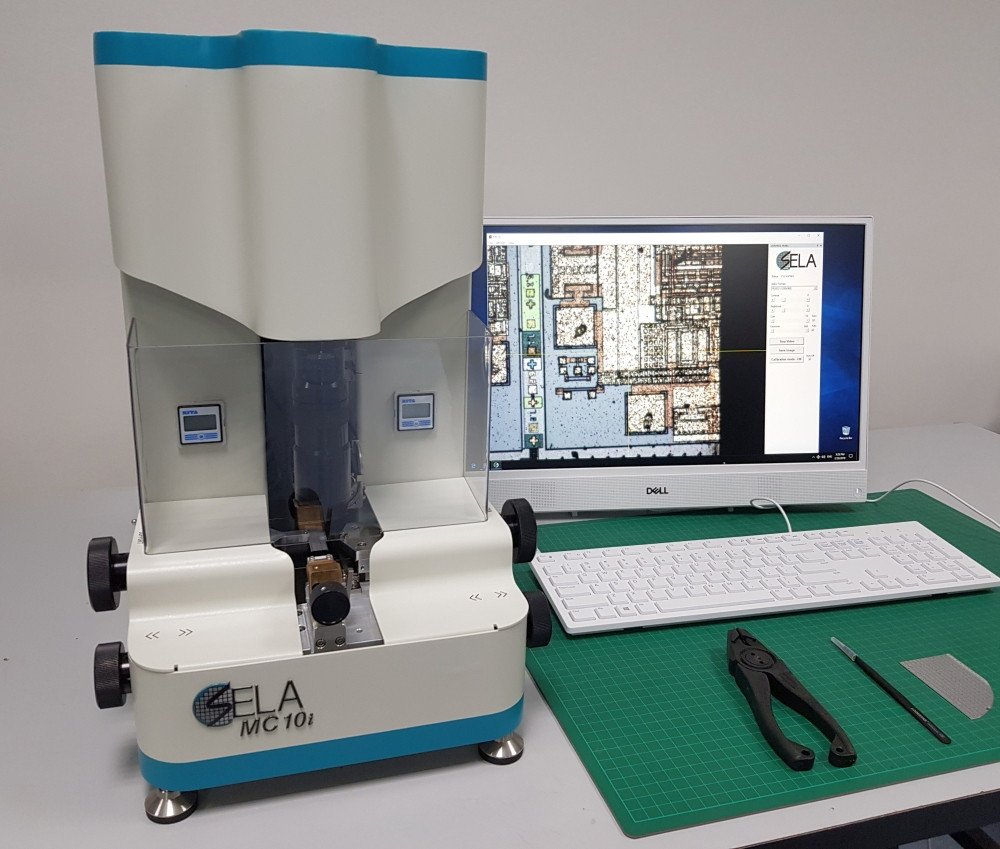
The SELA newest MC10i smart micro cleaving system with capability of liquid nitrogen spraying is the advanced solution for the SEM sample preparation of crystalline materials with high quality, high accuracy and high throughput. The MC10i utilizes and delivers to customers enhanced capabilities of wining SELA's Micro Cleaving technology. The MC10i smart table top system is the enhanced version of the MC10 platform equipped with liquid nitrogen spraying capability, achieves semi-automatic, reliable, repeatable and rapid cross-sectioning of wafer segments and dies with high cleaving accuracy. Liquid nitrogen spraying during the cleaving provides strong additional capability for the failure analysis by drastically improving quality of the cross-section of metal lines, hard resist layers, TSVs and other materials. Dedicated software enables the accurate positioning control and alignment of the cleaving elements. Cleaved samples are ready for immediate inspection and analysis. The set of the MC10i together with PCM and TMO features target marking, extraction of the initial sample and final cross-sectioning with high throughput, high consistent accuracy and the excellent natural lattice quality of the cross-sections produced. Such advanced capabilities of the set of the MC10i significantly reduce the turnaround time for failure analysis and process monitoring. ENHANCED CAPABILITIES: Controllable liquid nitrogen spraying during cleaving; High quality cross-sectioning of metals, resist and other materials; Prevention of pull out of materials during the cleaving. FEATURES: Semi-automatic controllable cleaving process; Accuracy better than 5 microns, mostly 2-3 microns; Process time – single minute; Extremally small input sample or die – down to 1×1 mm; Cleaving as close as 1 mm to the wafer or die edge; Continuous cleaving of multiple targets; Advanced optics with variable magnification up to 1000x; Software controllable cleaving process; Built-in vacuum; “Maintenance free” servicing model. BENEFITS: Turnaround time significantly reduced; Improves yield analysis; Improves characterization; Improves and enhances SEM and FIN utilization; Low cost of ownership.
CATEGORY
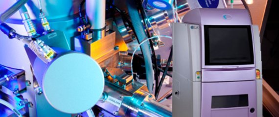
Xact200 performs cutting-edge TEM/STEM sample preparation in line with the Semiconductor and Nanotechnology roadmap requirements for next generation physical FA and characterization. The Xact200 is a second-generation system uniquely combines the disruptive innovative AIM technology with an integrated FE SEM column, in process real time STEM imaging capability and piezo based multi axes eucentric manipulator. The Xact200 delivers excellent sample quality, significantly reduced turn-around times and enhanced productivity. AIM, SELA’s proprietary Adaptive Ion Milling technology, is superior to traditional Focused Ion Beam (FIB) and Broad Ion Bean (BIB) technologies in ability to reduce lamella thickness below 15 nanometers over a large area with artifact-free quality, high precision, controlled thickness variation and high throughput. SYSTEM HIGHLIGHTS - Unsurpassed quality with negligible artifacts - Amorphous layer about 1nm on Si - Routine lamella thinning to below 20nm covering a wide area of interest - Thinning down to 10nm supporting 1x technology node - Enhanced lamella thickness uniformity and robustness - High precision milling with integrated FE SEM/STEM observation - AIM technology enabled by unique ion milling unit With dynamic Xe ion beam SYSTEM FEATURES - Side and Plan view TEM/STEM preparation - Top and back side Delayering - SEM cross-section preparation for wide and high structures - SCM and SSRM preparation - Preparation of extremely big and extremely small objects - TSV and bumps SEM and TEM/STEM preparation - Real time STEM imaging during the milling - Real time thickness measurement during the milling - Ease of use
CATEGORY
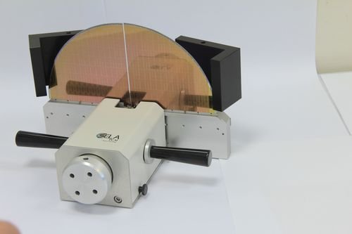
Perfect Cleave Mechanism (PCM) is a simple manual cleaving tool for cross-section of crystalline materials such as Si, GaN, GaAs, InPh, SiC and others. PCM utilizes SELA’s proprietary Perfect Cleaving technologies to achieve fast cleaving of crystalline materials with perfect quality of cross-section. The PCM had been presented to semiconductor market and delivered to customers in 2000 as a stand-alone solution for the sample preparation for SEM analysis and as a complementary tool for the initial sample preparation for the automatic nano cleaving series of SELA – MC500, MC600 and MC600i systems SELA’s customers recognized great capability of the PCM and utilized it for wide variety of preparation requirements for past 15 years. PCM is a compact tool and customers use it under magnified glasses and optical stereo microscopes to improve accuracy of cleaving. SYSTEM HIGHLIGHTS Perfect quality of cross-section High throughput Improves and enhances SEM imaging Compact size Low cost of ownership SYSTEM FEATURES Perfect quality of cross-section for crystalline materials Fast cleaving in less than a minute Size of cleaved samples from full wafer and to single die 2x2mm Manually controlled accuracy Ease of use – – no previous experience required
CATEGORY
