By California Nanotechnologies Corporation
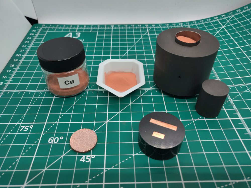
The ability to produce high-performance components quickly and with precision is critical. That’s where Spark Plasma Sintering (SPS) machines come into play. Also known as Field-Assisted Sintering Technology (FAST) or Pulsed Electric Current Sintering (PECS), SPS machines are revolutionizing the way powdered materials are transformed into solid, high-density parts. An SPS machine is a highly specialized piece of equipment designed to sinter powders—typically metals, ceramics, or composites—into dense, solid materials. It achieves this by applying uniaxial pressure and high-frequency pulsed electric current directly to the powder, generating heat through Joule heating and creating a plasma effect that rapidly fuses particles together. The sintering process occurs at lower temperatures and in significantly shorter timeframes compared to traditional sintering methods. Components are often consolidated within 5 to 30 minutes, versus hours for conventional furnaces. The entire process typically takes place in a vacuum or inert atmosphere, preserving the purity of the material. How Does It Work? 1. Powdered material is loaded into a graphite die. 2. The die is placed inside the SPS chamber. 3. A pulsed DC current is applied, generating internal heat. 4. Simultaneously, uniaxial pressure is exerted on the powder. 5. The heat and pressure cause rapid densification of the material into a near-net-shape solid part. Advantages of SPS Technology - Rapid Processing: Sintering takes minutes, not hours. - Lower Temperatures: Minimizes grain growth and energy usage. - Microstructure Control: Ideal for retaining fine structures, including nanomaterials. - Near-Net Shaping: Reduces waste and machining requirements. - Material Versatility: Effective for metals, ceramics, composites, and even difficult-to-process materials. SPS technology supports a wide variety of industries, each benefiting from its speed, precision, and versatility. Here’s how SPS is used across sectors: 1. Research & Development - Common in universities and national labs - Enables the testing and creation of new material combinations - Supports exploration of nanostructured and metastable materials 2. Powder Metallurgy & High-Performance Components - Used for sintering hard metals (e.g., tungsten carbide, molybdenum) - Produces parts for cutting tools, engine components, and molds - Common in aerospace, automotive, and heavy industries 3. Biomedical Applications - Produces bio-compatible implants (e.g., dental implants, bone scaffolds) - Materials like titanium, zirconia, and hydroxyapatite are popular - Helps create dense parts with minimal contamination 4. Advanced Ceramics & Electronics - Sintering of electroceramics, piezoelectrics, and solid oxide fuel cell components - Ideal for thermal barrier coatings, substrates, and heat-dissipating parts 5. Aerospace & Defense - Manufactures lightweight, heat-resistant components - Applications include armor plating, turbine blades, and heat shields - Favored for high strength-to-weight ratios 6. Energy Sector - Used for thermoelectric materials (e.g., bismuth telluride) - Supports battery development, fuel cell production, and solar technology - Enables higher efficiency and innovative energy storage solutions 7. Nanotechnology Applications One of the most significant advantages of SPS lies in its ability to preserve nanoscale features during sintering. Traditional sintering techniques often result in grain growth, which can diminish the unique properties of nanomaterials. SPS, however, sinters powders at lower temperatures and faster speeds, which helps retain the nanostructure and surface area of the original material. Nanotechnology-related uses include: - Nanostructured ceramics and composites with superior strength and toughness - Functional nanomaterials for electronics, catalysis, and photonics - Magnetic and thermoelectric nanomaterials with enhanced properties - Creation of functionally graded nanomaterials for next-gen devices This ability to control and maintain nanoscale features makes SPS indispensable in the fabrication of materials with tailored electrical, thermal, and mechanical behaviors—paving the way for innovations in microelectronics, sensors, batteries, and more. Who Uses SPS Machines? - Academic and Government Labs: For prototyping and materials discovery - Aerospace and Defense Contractors: For precision-critical, high-performance parts - Biomedical Companies: To produce patient-specific implants - Advanced Ceramics and Tooling Manufacturers: For ultra-hard, wear-resistant products - Nanotechnology Researchers and Startups: For developing next-gen materials and components Spark Plasma Sintering machines represent the cutting edge of modern manufacturing, providing unmatched speed, control, and versatility. Whether you’re producing ultra-hard tools, high-purity biomedical implants, or next-generation nanomaterials, SPS offers a powerful solution that meets the demands of both innovation and efficiency. As industries continue to seek lightweight, strong, heat-resistant, and nanoscale-optimized materials, SPS technology is poised to play a central role in shaping the future of advanced manufacturing and nanotechnology.
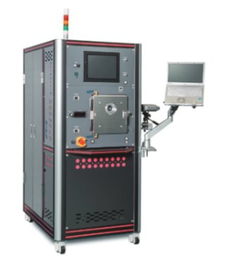
Our SUGA SPS2000 systems are optimized for research, development, and small-batch production. • Ideal for material screening and process development • Rapid heating and cooling capability • Advanced waveform and process control • Flexible tooling configurations • Excellent platform for early-stage prototyping These systems allow customers to quickly validate materials and transition efficiently toward production-scale processing. Here is a link to their brochure - SPS System Brochure Click Here for SPS System Video Demonstrations! Features: •DEGAS mode - to improve the purity of powder materials •RAPID COOLING mode – quick cycle time •SELECTABLE WAVE FORMS - DC Pulse, Full Wave and Continuous Wave and more…
CATEGORY
Cal Nano operates the Dr. Fritsch MSP-5, one of the largest commercially available SPS systems in North America. The MSP-5 significantly expands processing envelope and enables production-oriented manufacturing of large or high-volume components. • High force and high current capacity for aggressive sintering cycles • Large-diameter part capability • Designed for scale-up from R&D to manufacturing • Supports production volumes for aerospace, nuclear, defense, and energy applications • Enables consolidation of advanced ceramics, refractory alloys, MMCs, and specialty materials The MSP-5 allows Cal Nano to bridge the critical gap between laboratory success and commercial production.
CATEGORY
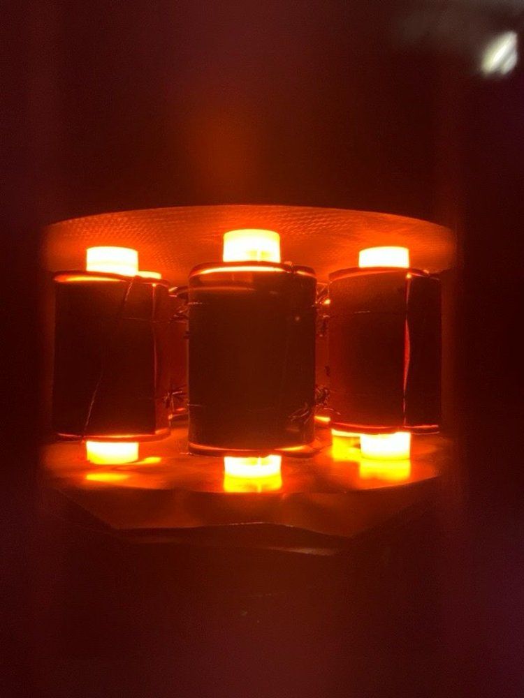
Cal Nano supports advanced nuclear and defense programs with refractory and specialty alloy processing designed for extreme service conditions. Materials and systems include: - Molybdenum-based alloys - Tungsten-based systems - Refractory composites - Metal-ceramic composites (MMCs) - SPS-bonded and diffusion-bonded assemblies These materials are engineered for high-temperature stability, thermal resistance, and demanding reactor and defense environments.
CATEGORY
Tungsten carbide dies are industrial tools used for shaping, forming, and compacting metals and other hard materials. These dies are composed of tungsten carbide — a composite material made of tungsten and carbon atoms — renowned for its extreme hardness and resistance to wear, deformation, and high pressure. At Cal Nano, we utilize this material to fabricate dies capable of handling even the most demanding industrial applications. Whether used for wire drawing, cold heading, powder compacting, or extrusion, our tungsten carbide dies deliver unmatched performance and longevity. Tungsten carbide is an ideal choice for dies due to its unique combination of hardness, strength, and wear resistance. With a hardness second only to diamond, it resists deformation and abrasion under extreme mechanical loads, making it indispensable in high-pressure or high-friction environments. Key Advantages: - Exceptional wear resistance - High compressive strength - Resistance to deformation and cracking - Dimensional stability under high loads - Extended tool life and reduced downtime These properties translate into significant cost savings, greater precision, and longer intervals between die replacements — all essential in high-volume or high-tolerance production environments. Wire Drawing: Used to reduce the diameter of metal wires by drawing them through a series of progressively smaller dies. Our tungsten carbide dies ensure high-speed wire drawing with minimal wear, perfect for steel, copper, and aluminum wires. Cold Heading and Forming: In the production of fasteners such as bolts, rivets, and screws, tungsten carbide dies withstand the immense pressures of cold forming without cracking or distorting — enabling cost-effective, high-volume production. Powder Compaction: For industries like automotive and aerospace, we design tungsten carbide dies used to compact metal powders into solid components before sintering. These dies offer the hardness and stability required to create high-strength parts with tight dimensional tolerances. Extrusion and Stamping: In shaping bars, rods, tubes, and profiles, tungsten carbide dies are essential for high-pressure extrusion and stamping applications. Their durability ensures consistent results even under continuous operation.
CATEGORY
