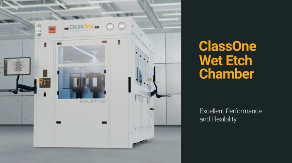
Our wet etch chamber is designed to deliver you high performance, better cost of ownership, and improved safety. Our flexible fluidics design allows for multiple chemistries to be plumbed to each of the chambers. Inline heaters can be used for fine temperature control <±0.5°C for many applications. Recipe-addressable drain blocks and filtration can be configured for efficient reclaim and introduction of fresh chemistry. Additionally, optical endpoint detection can be used to dynamically adjust etch time and ensure precision film removal. The face-down orientation of our chambers seals the chemistry in the chamber and prevents operator exposure. Our wet etch chambers can be combined with segregated face-up SRD chambers for cleans applications. The face-up SRD draws clean air directly from the HEPA filters, which aids in a speedy and clean dry that is segregated from the wet etch chambers. Enjoy great performance and safety with the Solstice®wet etch chamber. Capabilities - UBM Etch - Metal Etch - Seed and Barrier Etch - Oxide Etch - Silicon Etch - TSV Cleans - RCA–SC1 Cleans
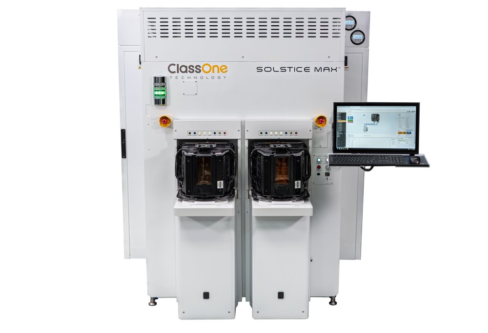
Modular Single-Wafer Processing for 200mm and 300mm Wafers The Solstice® Max platform extends ClassOne's proven single-wafer wet processing technology into a new era of modularity. Purpose-built for a broad range of wafer-level packaging (WLP) applications and fab types. Solstice Max delivers advanced electroplating and surface preparation performance with the ability to process both 200mm and 300mm wafers in the same tool. Designed from the ground up to deliver low cost of ownership (CoO), Solstice Max offers unmatched price-to-performance, process flexibility, reliability, and extraordinary modularity that grows with your production needs. Modular, Scalable Architecture The Solstice Max platform is precision-engineered to deliver process performance for today's most advanced packaging requirements with exceptional flexibility: - 200mm & 300mm capability in one platform – run silicon, glass, thinned, and bonded wafers of both sizes concurrently. - Modular, field-extendible design – start with a four-chamber system and add four-chamber modules, to a maximum of four modules (16 chambers), as production ramps. - Compact footprint – enables Solstice Max to be installed in a wide range of cleanroom environments and can accommodate fabs with height limitations. - Unbeatable ROI – achieve exceptional on-wafer results and throughput without unnecessary complexity. Multiple Processes for Expanded Possibilities Solstice Max provides a turnkey solution for electroplating, wet processing, solvent strip, and wafer cleans — allowing customers to configure unique process flows within the standard framework of the platform. Key Applications Solstice Max targets six key vital plating and wet surface process applications that encompass a host of capabilities: Advanced Packaging • High-value electroplating and support processes for advanced packaging and other back-end applications such as bumping, pillar, and multi-metal stacks. • Enabled by high-performance, fountain-style plating chamber design, together with vacuum pre-wet, wet-etch and other wet processing chambers. Seed & Barrier Etch • Fast, uniform application of seed & barrier etch chemistries enabled by the wet-etch chamber with face-up SRD. • End point detection allows for automatic recipe optimization and ongoing process validation. Solvent Processing • Dedicated or partial solvent tools can be configured with PR strip and metal liftoff (MLO) chambers, using both flood-soak and high-pressure swing arm, enabled by face-down architecture. • Stainless steel chamber design that is closed and exhausted during process, allows for safe handling and use of solvent chemistries, while minimizing escape of vapors and fumes. Back-End Cleans • Single-wafer solvent, wet-etch and bevel-etch chambers provide the full suite of options for targeted back-end cleans. • Solstice performs fast, efficient backside and front-side cleans at many steps within back-end processing to ensure wafer and packaging integrity. Advanced Gold Plating • Gold plating is the established standard for many applications, especially VCSEL and RF devices • The ECD chamber design enables rapid deposition with excellent uniformity across device types. • The Solstice Max platform's chamber flexibility is ideally suited for developing and scaling new technologies – from glass and microLEDs to hybrid bonding, heterogeneous integration, and more.
CATEGORY
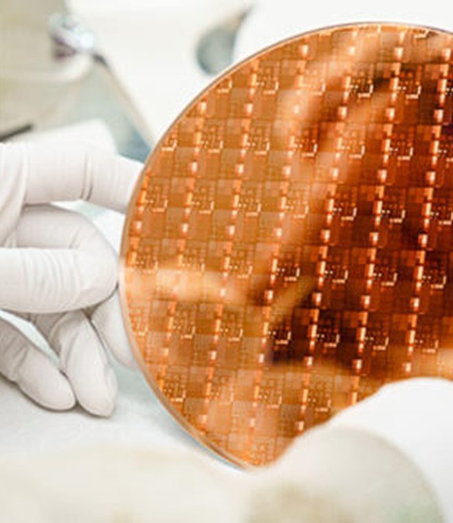
ClassOne’s Solstice is a great match for the advanced packaging market. From market leaders to new entrants in Europe and Asia, ClassOne serves these customers with its highly flexible Solstice platform. Combining advanced high-performance plating and surface-prep chambers allows both high-volume and specialty/niche packaging partners to process wafers. Our customers continue to advance processes in pillar, TSV, RDL, interposer and other emerging interconnect technologies such as hybrid bonding. From VCSEL sensors to advanced AI communication chips, Solstice serves the photonics market. In handling fragile indium phosphide (InP) and gallium nitride (GaN) wafers, Solstice uses automation that can easily adapt to different wafer sizes and types. Additionally Solstice takes advanced process technology that is usually only available for large wafer types (300mm) and scales it down effectively to 3-, 4-, 6-, and 8-inch wafers. With AI data centers continuing to increase, the need for fast, low-latency, high-bandwidth data communication shows no sign of abating, heightening the need for Solstice’s proven performance. In AI, indium phosphide (InP)-based photonic transceiver technology is needed to build bigger and better AI data centers. Connecting thousands of GPUs for large neural net training batches requires fiber-optic technology and advanced transceivers to transfer data effectively. Solstice’s ability to handle 3-, 4-, and 6-inch Indium Phosphide (InP) wafers and provide advanced, fully automated processing sets it apart in the marketplace. Additionally, Solstice’s class-leading gold plating and metal lift-off process (MLO) technology gives fabs the ultimate value in metallization. MEMS device makers appreciate ClassOne’s Solstice for its flexibility and capability in diverse processing applications. As a variety of product types continue to be introduced to support IoT and smart devices, fabs need a tool that can be easily modified to support new wafers and processes. ClassOne’s modular tool design and flexible design orientation gives it unmatched capability to support customers in this segment. In RF and power, Solstice’s capability to provide high-volume gold-plating processes is widely leveraged. Device makers in this segment appreciate the system’s elegant design, which makes it easier to service and faster to dial-in uniformity. All of this is enabled without sacrificing performance or operating costs. The Solstice tool uses an advanced fountain plater design with in situ rinse to preserve bath chemistry and give customers uncompromised cost and performance. The Solstice platform enables high-precision processes like through-silicon via (TSV), hybrid bonding, and interposers for advanced packaging, while also enabling uniform fast plating for VCSELs, microLEDs, and RF filters used in 5G communications.
CATEGORY
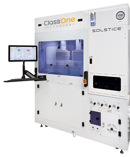
ClassOne Technology's Solstice single-wafer platform is affording new opportunities for universities and research institutions to up their manufacturing game at an attractive cost The Solstice platform is uniquely suited to serve as the bridge tool from wet bench to single-wafer processing for universities, as well as research institutions. Specifically designed for electroplating and surface preparation processes, Solstice provides the ability to configure an AP cluster system, where plating, photoresist strip and wet etch are all performed on one tool with a highly compact footprint. One example of the technologies that universities are researching is ultra-high-aspect-ratio through-silicon via (TSV) features on semiconductor wafers, for which Solstice Vacuum Pre-Wet and CopperMax chambers allow universities to continue pushing the aspect-ratio boundary. Additionally, universities are delving into new areas like quantum computing; here, Solstice is able to handle novel processes and unique materials in advanced applications, including indium and aluminum. Solstice is available in three primary models that can be configured in numerous ways to process virtually any type of wafer substrate from coupon to 200mm in diameter: - LT, with up to three chambers, is a manual system ideally suited for low-volume/R&D using the same chamber architecture as the automated systems. - S4, with four chambers suited to pilot production and robotic wafer handling, allows students the opportunity to gain experience in programming automation. - S8 features up to eight chambers, also with automated wafer handling, enabling plating and surface preparation for a fully integrated AP process on one tool. All three systems deliver the same superior process control and uniformity at the lowest capital costs by comparison. ClassOne is seeing interest in all three models from various schools, with the Solstice LT leading the way as the ideal option for economical entry to single-wafer processing. Because the tool is easy to install and operate, students can be up and running quickly. With its low cost of entry, low cost of ownership and ease of maintenance, it offers an attractive sweet spot for university implementation.
CATEGORY
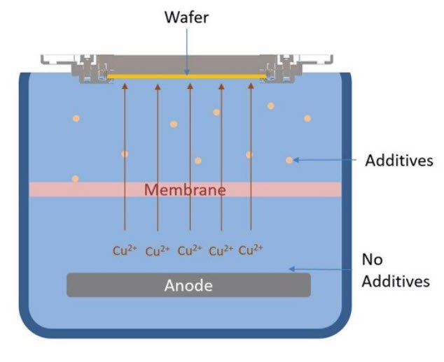
Modern semiconductor copper plating chemistries include expensive, highly engineered organic additives that serve to enhance the quality of the plating. However, these additives are readily destroyed when they come in contact with the copper anode of the plating system. This necessitates ongoing replenishment of additives and significantly increases process costs. Our proprietary Solstice®CopperMax™ chamber integrates a cationic exchange membrane that separates organic additives from the anode while still allowing high-speed copper cation movement to the wafer. This enables higher plating rates while routinely reducing the user's chemistry costs by more than 95% – and also delivering excellently plated feature uniformity. Eliminating Additive Breakdown The proprietary design of our Solstice CopperMax chamber dramatically reduces the deterioration of organic additives by using a cationic exchange membrane to keep additives from contacting the anode. This significantly reduces your chemistry costs while enhancing copper plating quality. In other chambers, the plating behavior shifts rapidly as additives break down. The bath metrology begins to return inaccurate readings, which leads to erroneous dosing. Applications - Wafer level packaging - Flip-chip interconnects - Solder bumping (with nickel & solder plating) - C4 bump - Thermo-compression bonding - And more… Features - Cation exchange membrane to reduce additive use - Continuously filtered chemistry, optional carbon filtration - High-precision wafer rotation - Adjustable diffuser - Dry-contact, low-maintenance plating rotor - Customized seal reach - Levitronix pump with LeviFlow Benefits - Additive costs reduced 95% - Maximized bath life - Extremely uniform field profile - Seal reach aligns to existing integration - Continuously cleaner chemistry - Precise, consistent flow rate control Technical Data Wafer Materials Silicon, GaAs, GaN on Si, GaN on Sapphire, Sapphire, Transparent Substrates, and more Flow Rate 25 lpm Plating Rate 3μm/minute, up to 6.5μm/minute Within-Wafer Uniformity<3% (range 2mean) Wafer-to-Wafer Uniformity<1% (mean-to-mean) CD Reduction<0.2Å on 1200Å seed deplate Coplanarity<5%
CATEGORY
