Our highest-purity nanotube-based semiconducting ink leads to printed or etched transistors with remarkable mobility and ON/OFF ratio that are used for sensing applications. Our inks were used for over one hundred scientific publications in the last 2 years and are now being tested in late-phase industrial R&D programs. Our latest polymer-wrapping separation technology, licensed from the NRC, bypasses our previous bottleneck to mass scale-up. Our semiconducting and conducting inks are also tested for logic, photovoltaics, anti-counterfeiting and biomarkers, among other applications.

These single-wall carbon nanotubes are purified to values of 95-98% (nanotube content measured via the Itkis ratio). PureTubes offer metal content lower than 5% metal content (as per TGA). These are our highest purity un-sorted nanotubes. Sourced from the arc-discharge processes and offered in solution or dry powder. Characterisation Optical Absorbance Figure 1. Optical absorbance plots for our PureTubes. Following the method of Ouyang et al. (Acc. Chem. Res. 35, 1018 (2002)), we can calculate the transition energies for nanotubes in our diameter range (1.2 – 1.7 nm). We see peaks where we would expect them: S33 transitions should lie between ~450-630 nm, M11 transitions between ~600-850 nm, and S22 transitions between ~ 900-1,270 nm. We estimate our SWCNT purity by the ratio of the S22 peak area (after linear background subtraction) to the total area in the band (Itkis et al. JACS (2005) 127, pp 3439-3448). Before comparison, the individual peak areas are scaled by empirically determined values for the M11 and S22 extinction coefficients. Metal Catalyst Neutron Activation Analysis Nickel (wt %): Unprocessed SWNTs 3.59, PureTubes 0.23 Yttrium (wt %): Unprocessed SWNTs 0.70, PureTubes 0.05 Iron (wt %): Unprocessed SWNTs 0.70, PureTubes 0.06 Total (wt %): Unprocessed SWNTs 4.99, PureTubes 0.34 Iodine (wt %): Unprocessed SWNTs 0.00, PureTubes 0.00 Full elemental profiles of our products are available upon request. Figure 2. Neutron activation analysis (NAA) data taken from our unprocessed and PureTube powders. NAA reveals that our PureTubes contain significantly lower levels of metallic/catalyst impurities than the raw arc discharge SWNTs from which they are produced. Metal Catalyst Thermogravimetric Analysis Figure 3. Thermogravimetric (TGA) plots of our nanotube products. Because our PureTubes do not contain iodixanol, the burnoff of residual surfactant and amorphous carbon is solely accountable for the ~5% mass decrease which occurs between approximately 200 and 400°C. Amorphous Carbon Raman Figure 4. Resonance Raman plots for our PureTubes. All Raman measurements were taken using a 514 nm laser. The G/D ratios of our products range from approximately 12 to 41, indicating extremely low levels of amorphous carbon and/or damaged nanotubes. Length Atomic Force Microscopy Figure 5. Atomic-force microscopy (AFM) data indicates that our SWNTs range in length from approximately 100 nm to 4 microns. Length histograms of our PureTubes. Properties at a Glance Nanotube Type: Arc discharge (Manufacturer data) Diameter Range: 1.2 – 1.7 nm (Manufacturer data) Mean Diameter: 1.4 nm (Manufacturer data) Length Range: 100 nm – 4 μm (AFM) Mean Length: ~1 micron (AFM) Catalyst Impurity: ~0.5% by mass (NAA, TGA) Carbonaceous Impurity: < 5% by mass (TGA, Raman) Semiconducting CNT Content: n/a (Optical absorbance) Metallic CNT Content: n/a (Optical absorbance) Shelf Life: 6 months Nanotube Concentration: 0.25 mg/mL Surfactant Concentration: 1% w/v Surfactant Type: Ionic (proprietary mixture)
CATEGORY
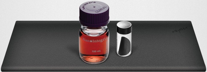
High Purity Semiconducting Nanotubes IsoSol-S100 / sc-SWCNT A semiconducting carbon nanotube ink with the highest purity ever measured coupled to a fully scalable manufacturing route: IsoSol-S100. The semiconducting single-wall carbon nanotubes are sourced from the highly-scalable RF-plasma grown carbon nanotubes, and separated using a conjugated polymer extraction process. Product Summary The use of specialized patent-pending dialkyl homopolymers developed by the National Research Council of Canada within the Printable Electronics Consortium, has enabled us to disperse and extract single-walled carbon nanotubes to the highest levels of semiconducting enrichment and purity to date: IsoSol-S100. The starting materials are the purified and highly-scalable RF-plasma grown carbon nanotubes supplied by Raymor Nanotech. UV-Vis-NIR spectrophotometric assessment of purity indicate that this material has semiconducting purities at or greater than 99.9% with the metrics of Itkis Ratio and Phi Values exceeding 0.5 and 0.4, respectively. The highly graphitized starting material and low sonication intensity utilized for the extraction technique minimizes damage to the nanotubes, allowing the material to exhibit high crystallinity and longer average lengths of 1μm, not previously seen when utilizing DGU or Chromatography-based separation methods. Additionally, the material is processed in organic solvent and the polymer/nanotube ratio can be adjusted to less than a factor of four with nanotube concentrations 10x higher than our aqueous dispersions. The solutions also display stabilities of greater than six months. These properties promote great nanotube deposition and adhesion for device creation. Experimentally, thin film transistors, prepared on SiO2/Si substrates have led to average mobilities exceeding 27cm2/(Vs) and On/Off ratios of 1.8×10⁶ and is perfectly-suited for commercial ink jet and aerosol jet printing. Product Specifications Optical Purity 99.9% Itkis Ratio (Ї) 0.5 Phi Value (Φ) 0.39 Nanotube Concentration 0.01mg/mL Surfactant: Nanotube Concentration <4 Standard Solvent Media Toluene Shelf Life 6-9 months SEM and AFM Diameter Range 1.2 – 1.4 nm Mean Length 1 μm Raman The Radical Breath Mode (RBM) of the spectra excited at 785nm shows that the IsoSol-S100 material has a nearly flat baseline in the metallic region from 145 to 175 cm-1, indicative of a high semiconducting purity. Metal Catalyst Impurity <0.5% Amorphous Carbon Impurity PLE Map A photoluminescence excitation (PLE) map for the IsoSol-S100 material shows well resolved (S 22,S 11) maxima, indicative of well separated nanotubes. UP to 19 (n,m) species contribute to the spectrum, with 8 or 9 having peak intensities higher than or close to 0.5. The (10,9) chirality peak with S 11=1570nm and S 22=910nm, proved to be the strongest. For further details, reach out to our Sales Manager at sales@raymor.com or call +1 450.434.6266. Large volume discounts available for large quantities. Please contact us for more information. IsoSol-S100 Technical Data Sheet NanoIntegris supplies premium nanomaterials to companies and academic institutions developing next-generation electronics, energy, and biomedical technologies.
CATEGORY
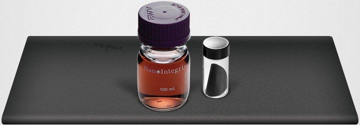
Semiconducting single-wall carbon nanotubes are a NanoIntegris exclusivity. Sorted using our patent density gradient ultracentrifugation (DGU) process. Offered in an acqueous solution or a powder. Electronic Type Enrichment - Optical Absorbance: Figure 1. Optical absorbance plots for our IsoNanotubes-S (99%), respectively. Following the method of Ouyang et al. (Acc. Chem. Res. 35, 1018 (2002)), we can calculate the transition energies for nanotubes in our diameter range (1.2 – 1.7 nm). We see peaks where we would expect them: S33 transitions should lie between ~450-630 nm, M11 transitions between ~600-850 nm, and S22 transitions between ~ 900-1,270 nm. We estimate our metallic and semiconducting enrichment levels based on ratios of the M11 and S22 peak areas after linear background subtraction. Before comparison, the individual peak areas are scaled by empirically determined values for the M11 and S22 extinction coefficients. Metal Catalyst - Neutron Activation Analysis: Unprocessed SWNTs: Nickel (wt %) 3.59; Yttrium (wt %) 0.70; Iron (wt %) 0.70; Total (wt %) 4.99; Iodine (wt %) 0.00. IsoNanotubes-M + S: Nickel (wt %) 0.07; Yttrium (wt %) 0.38; Iron (wt %) 0.72; Total (wt %) 1.17; Iodine (wt %) 5.29. Full elemental profiles of our products are available upon request. Figure 2. Neutron activation analysis (NAA) data taken from our IsoNanotube and PureTube powders. NAA reveals that our IsoNanotubes and PureTubes contain significantly lower levels of metallic/catalyst impurities than the raw arc discharge SWNTs from which they are produced. Our IsoNanotube samples, however, contain approximately 5% iodine by mass, resulting from residual iodixanol on the surface of the nanotubes that is not eliminated by our surfactant removal procedures. Metal Catalyst - Thermogravimetric Analysis: Figure 3. Thermogravimetric (TGA) plots of our nanotube products. Approximately 2/3 of the ~15% mass decrease which occurs between ~200 and ~400°C is attributable to the burno! of residual iodixanol adsorbed to the surface of the nanotubes. NAA data indicates that our IsoNanotubes contain roughly 5% iodine by mass (see Figure 3); iodine comprises roughly half the mass of an iodixanol molecule. The remaining 5% mass decrease is attributable to the burno! of residual surfactant and carbonaceous impurities. Amorphous Carbon - Raman: Figure 4. Resonance Raman plots for our IsoNanotubes-M (95%). IsoNanotubes-S (99%), and PureTubes, respectively. All Raman measurements were taken using a 514 nm laser. The G/D ratios of our products range from approximately 12 to 41, indicating extremely low levels of amorphous carbon and/or damaged nanotubes. Length - Atomic Force Microscopy: Figure 5. Atomic-force microscopy (AFM) data indicates that our SWNTs range in length from approximately 100 nm to 4 microns. Length histograms of our IsoNanotubes-M respectively. Properties at a Glance: Nanotube Type: Arc discharge (Manufacturer data); Diameter Range: 1.2 – 1.7 nm (Manufacturer data); Mean Diameter: 1.4 nm (Manufacturer data); Length Range: 100 nm – 4 μm (AFM); Mean Length: ~1 micron (AFM); Catalyst Impurity: ~1% by mass (NAA, TGA); Carbonaceous Impurity: < 5% by mass (TGA, Raman); Semiconducting CNT Content: 90%, 95%, 98%, or 99+% (Optical absorbance); Metallic CNT Content: n/a (Optical absorbance); Shelf Life: 6 months; Nanotube Concentration: 0.01 mg/mL; Surfactant Concentration: 1% w/v; Surfactant Type: Ionic (proprietary mixture). For further details, reach out to our Sales Manager at sales@raymor.com or call +1 450.434.6266. Large volume discounts available for large quantities. Please contact us for more information. IsoNanotubes-S Technical Data Sheet
CATEGORY

Metallic single-wall carbon nanotubes are a NanoIntegris exclusivity. Sorted using our patent density gradient ultracentrifugation (DGU) process. Offered in an acqueous solution or a powder. Property | IsoNanotubes-M - Nanotube Type: Arc discharge; Diameter Range: 1.2 – 1.7 nm; Mean Diameter: 1.4 nm; Length Range: 100 nm – 4 μm (AFM); Mean Length: ~0.5 micron (AFM); Catalyst Impurity: ~1% by mass (NAA, TGA); Carbonaceous Impurity: < 5% by mass (TGA, Raman); Semiconducting CNT Content: n/a (Optical absorbance); Metallic CNT Content: 70%, 95%, 98% or 99% (Optical absorbance); Shelf Life: 6 months; Nanotube Concentration: 0.01 mg/mL; Surfactant Concentration: 1% w/v; Surfactant Type: Ionic (proprietary mixture) For further details, reach out to our Sales Manager at sales@raymor.com or call +1 450.434.6266. Large volume discounts available for large quantities. Please contact us for more information.
CATEGORY
