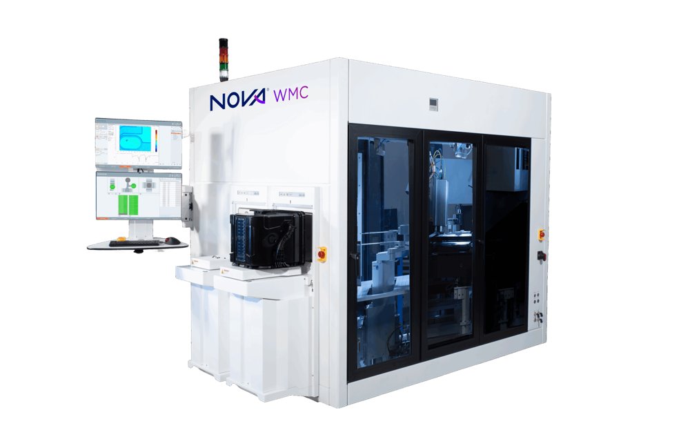
Next Generation Modular Optical Metrology Platform for Advanced Packaging Nova WMC is a high-end optical metrology platform designed to support 2.5D and 3D Advanced Packaging processes. Through the highly versatile modularity of its advanced metrology, handling, and loading systems, it combines precision, accuracy, and high throughput for outstanding performance at an unmatched Cost of Ownership. The platform’s unique ability to address major challenges such as high warpage, non-symmetric shapes, and different surface conditions, all in one tool, makes it the ultimate choice for 2.5D/3D packaging and HBM manufacturers. Highlights and Benefits Powerful Metrology Utilizing a range of high-end optical sensors (Interferometry, Reflectometry, and more), Nova WMC can serve as a cross-process, one-stop metrology solution (e.g., HBM manufacturing) Outstanding Performance Nova WMC combines fast, repeatable scanning with large-area mapping at nanometer fidelity and uses adaptive focus technology for stable measurements on warped or non-uniform surfaces. Versatile Handling Designed to support different wafer sizes, framed wafers, and panels. With customizable load port configurations and end effectors, Nova WMC can handle multiple advanced packaging scenarios. Automated Workflows With SEMI-compliant connectivity, it integrates seamlessly into fabs’ automation environments, while supporting automatic recipe loading and centralized recipe management for efficient operation. Future Ready Nova WMC’s future-ready metrology technology, together with its highly flexible system design with in-field upgrade capability, supports the evolving process challenges and customer needs. Why Nova WMC? Nova WMC redefines wafer metrology for advanced packaging by delivering a unified solution to the most complex challenges in 2.5D/3D integration and HBM manufacturing. Built on a modular, future-ready architecture, it seamlessly adapts to evolving process demands while maintaining exceptional precision and throughput. Its unique multi-sensor approach—featuring in-house-developed optical technologies—enables accurate, repeatable measurements across diverse surface conditions, including warped or non- uniform surfaces. Nova WMC’s versatility extends to handling a wide range of wafer sizes and formats, ensuring compatibility with the full spectrum of advanced packaging workflows. With robust automation, SEMI-compliant integration, and scalable performance, Nova WMC empowers fabs to accelerate yield, reduce cost of ownership, and confidently navigate the next generation of semiconductor innovation. Applications Backside Silicon Thickness Pre / post grind and post CMP Silicon thickness, c overing a range of 1 to 1000 µm. H igh-throughput measurements with full wafer mapping for complete thickness profile analysis. Wafer Warpage Detailed full-wafer warpage mapping provides a comprehensive view of wafer deformation. Bow measurements are performed at selected key points to quickly assess wafer curvature. Bond Layer TTV Single-layer measurements can be performed on multi-layer samples, such as the adhesive bond layer between the wafer and the carrier. Bonding eccentricity is also detectable for alignment analysis. Topography Analysis Geometric parameters such as C ritical D imension (CD), height, and distance can be measured, including features like RDLs, bumps, and laser grooves. Die Warpage (3D, D2W) Die warpage and thickness can be measured, typically in cases like framed wafers after dicing. Key results include metrics such as SFQR, SBIR, and others. Planar Thin Film Fast full-wafer mapping enables efficient measurement of thin film thickness and calculates the Total Thickness Variation (TTV) across the entire wafer. The measurement instrument can evaluate the thickness of up to four thin layers, down to 5 nm, either on test windows of a product wafer or across a blank wafer.
Next-generation solution for fast, high-precision inline XPS and XRF materials metrology Revolutionizing inline materials metrology, the Nova VeraFlex® LE-XRF product line is the industry standard for combined XPS and low energy XRF (LE-XRF) materials characterization. The most recent addition to the product line, Nova VeraFlex® IV LE-XRF addresses critical industry challenges across all device market segments. Higher precision and throughput are achieved by significantly increasing X-ray flux at the measurement site and integrating complementary machine learning solutions, enabling this next-generation platform to further strengthen the market leadership of the Nova VeraFlex® LE-XRF product line. Highlights and Benefits Higher Flux - System enhancements have been developed for increasing X-ray flux that generates higher photoelectron count rates and faster processing. This offers substantial throughput improvements while maintaining precise measurement performance. Measurements Where You Need It - Designed with enhanced X-ray beam alignment and control for smaller next-generation pad sizes, in-line measurements can be taken both in the scribe line and in-die on-device. XPS/XRF Sensitivity - Both XPS and LE-XRF measurements can occur simultaneously for inline and in-die applications, offering unique metrology solutions for critical yield-driving applications. Automated Health Check - Beam parameters from the electron gun and the generated X-ray beam energy are continuously monitored enabling uninterrupted high-volume manufacturing. Machine Learning - Machine learning capabilities enhancing the throughput and precision performance of new or established applications and maximize system productivity. Why VeraFlex® IV LE-XRF New material integration strategies continue to drive critical device performance improvements for advanced FinFet, Nanosheets, and novel memory structures. The VeraFlex IV LE-XRF provides the highest X-ray flux available to deliver the speed, sensitivity, and flexibility necessary to enable these performance breakthroughs.
CATEGORY
Advanced performance IM solution Nova i550® is a cutting-edge integrated metrology platform that provides superior metrology performance for CMP and etch process control in the most advanced logic and memory technology nodes Highlights and Benefits 01 Best Metrology Performance 02 Direct Device Measurements 03 Highest Productivity Best Metrology Performance Unique hardware and modeling capabilities that enable enhanced metrology performance Direct Device Measurements Measures logic and memory in-die structures, including complex 1D, 2D, 3D and direct devices Highest Productivity Faster throughput delivers better productivity Why Nova i550®? Nova i550® is designed to meet the process control challenges of the most advanced R&D developments and production lines. With new optics providing wider spectral information, a smaller pad size, and advanced pattern recognition to optimally support unique modeling algorithms, Nova i550® offers the industry’s highest metrology accuracy, precision and tool matching capabilities. Working in conjunction with the Nova MARS software application development platform, Nova i550® delivers advanced process control for the most advanced logic, 3D NAND double-deck structure, and advanced DRAM applications. Addressing the need for high-performance metrology closer to the process, Nova i550® significantly boosts productivity. Qualified for integration with leading vendors’ CMP and etch process equipment, the solution enables high sampling and multi-site measurement schemes. When supported by Nova’s central management, control and connectivity suite, Nova i550® offers even greater operational efficiency and advanced metrology control functionality.
CATEGORY
High-productivity metrology platform Nova T500® is a high-productivity metrology platform designed to address the unique challenges of the semiconductor manufacturing industry. The powerful platform delivers increased sampling rates and advanced metrology capabilities. Highlights and Benefits Industry Standard, Field Proven Platform Sets the industry standard for CMP process control, with thousands of deployments and proven reliability at customer sites, with optional field upgrades to further increase productivity Outstanding Performance Best-in-class accuracy, repeatability and tool-to-tool performance 100% Compatible to Nova i500® Utilizing the same design Engineering Station Supporting IM Product Line Used for recipe creation and as a redundancy tool that enables Pre/ Post measurement for additional sites and data collection Why Nova T500®? Nova T500® helps manufacturers meet the growing need for high productivity in advanced semiconductor manufacturing. Featuring the same optical design and having full commonality with the Nova i500® integrated metrology platform, Nova T500® completes the company’s unique, highly efficient CMP metrology and process control offering. As part of Nova’s fleet solution for semiconductor manufacturers, Nova T500® is qualified to support a broad range of tools, including Nova i500®, and is available in multiple configurations. When supported by Nova’s central management, control and connectivity suite, Nova T500® platform enhances operational efficiency and advanced metrology control functionality.
CATEGORY
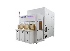
Nova Metrion® leverages secondary ion mass spectrometry (SIMS) technology to provide information that no other inline metrology system can deliver. This includes direct, inline measurement of chemical composition at high depth resolution and data density, as well as simultaneous measurement of multiple species throughout a 300mm wafer’s film stack. Process automation with built-in film analysis and recipe management makes the Nova Metrion® system easy to use, while performing these measurements in the production fab shortens time to results. Highlights and Benefits Direct Composition Profiling Directly measures compositional profiles inline at high depth resolution and data density Built-in Film Analysis Simplifies measurements and accelerates process insight with built-in film analysis and recipe management Full Factory Automation Supports full factory automation to enable high-volume manufacturing Contamination Free Ensures worry-free use within contaminant-sensitive production environments Whole Wafer Measurements Eliminates sample preparation and enables multi-point measurements for wafer uniformity mapping Reduced Scrap and Enhanced Yield Faster time to results reduces scrap and improves yield to deliver fast return on investment (ROI) Why Inline SIMS? Delivering time-sensitive information needed to monitor and control high-volume manufacturing (HVM) workflows, inline SIMS prevents scrap, reduces rework,and enables tighter statistical process control (SPC).
CATEGORY
