By NenoVision
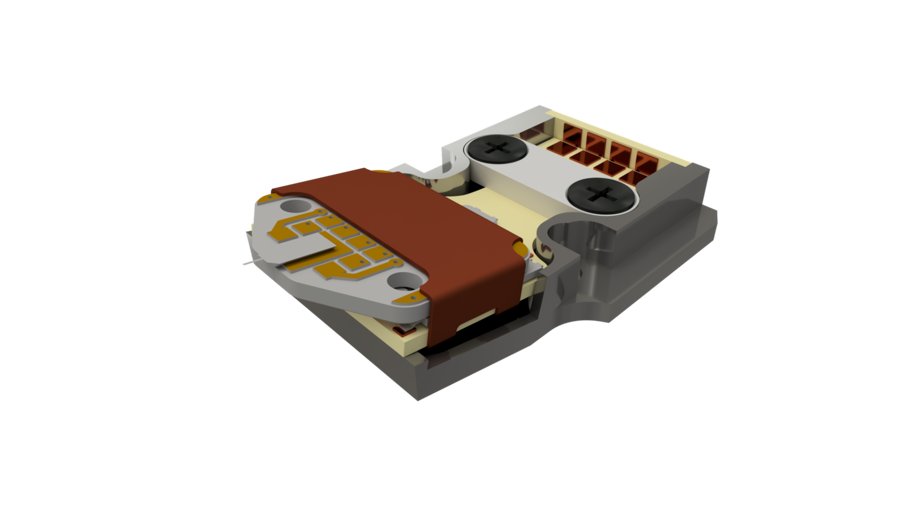
AFM-in-SEM LiteScope. Merge the forces of AFM and SEM. Site-specific Delayering Tip Navigation. Failure Analysis with AFM-in-SEM LiteScope integrated directly into the FIB/SEM environment, enables in-situ, site-specific electrical and topographical characterization of semiconductor components at the nanoscale level. It delivers precise conductivity mapping and dopant profiling without compromising sample integrity. Key benefits and features: - Site-specific failure analysis: Providing high-resolution conductivity & dopant mapping while using SEM for precise localization. - Seamless in-vacuum workflow: Fully compatible with existing FA tools and workflows, preventing surface oxidation and contamination. - Probe protection & optimized access: Docking station preserves AFM tip during FIB milling, while sample rotation optimizes angle for accessing even complex geometries. - Time-Saving & Cost Efficient: Integrated solution reduces measurement time per sample and accelerates R&D. LiteScope solution for Semiconductor Failure Analysis: Our groundbreaking AFM-in-SEM solution enables in-situ, site-specific, high-resolution electrical property mapping of complex semiconductor devices, while allowing faster and more accurate failure localization at the interconnect level. This approach helps identify failure mechanisms more effectively, which can lead to enhanced device performance, greater reliability, and increased manufacturing yield. - Innovative in-situ correlative failure analysis approach - Time to result significantly reduced - Site-specific vias or transistors NenoVision combines tradition and expertise with unique solutions in nanoscale using AFM-in-SEM microscopy. Failure Analysis techniques from SEM (EBIC, EBAC, …) and AFM (C-AFM, SSRM, …) enhance defect detection and accelerate the failure diagnostics. Setup is compatible with SEM systems produced by Thermo Fisher Scientific, TESCAN, ZEISS, Hitachi, Jeol, and their accessories.
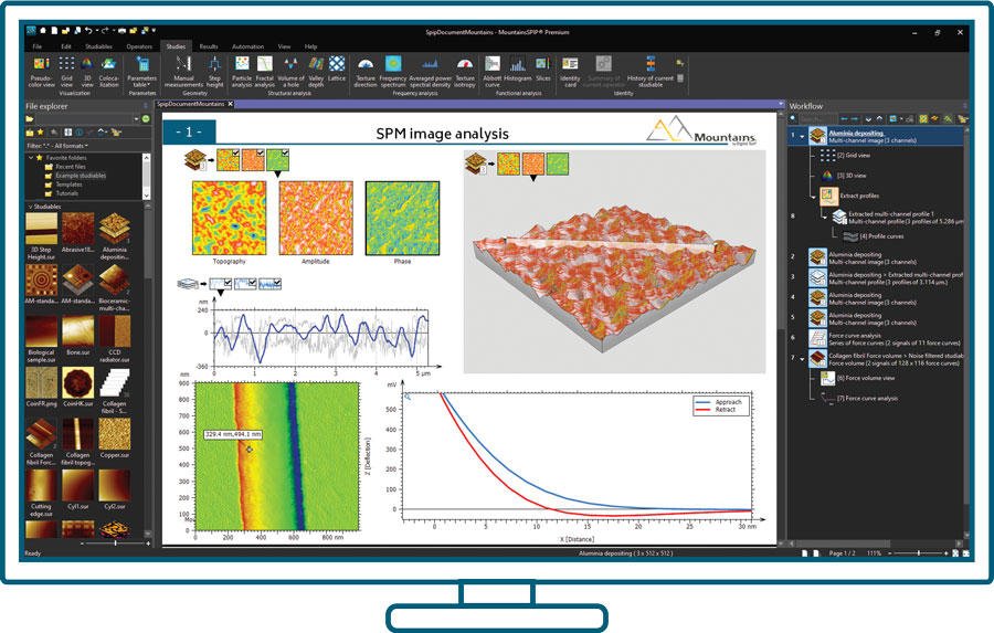
Key features of MountainsSPIP® software: - Interactive particle analysis: detect, quantify, and classify structures of any shape and size. - Force curve and force volume image analysis: analyze force curves and force volume images with precision and ease. - Correlative analysis: seamlessly combine your AFM data with data from your SEM. - Multi-channel file analysis: easily handle and analyze multi-channel files, simplifying complex data processing. - Data enhancement: correct, normalize, and denoise your measured data to extract meaningful insights. - Accurate XY calibration: ensure precise XY calibration for precise measurements and analysis. - Tip effect correction: correct for tip effects to enhance the accuracy of your results. - Surface texture characterization: investigate surface texture in compliance with ISO standards.
CATEGORY
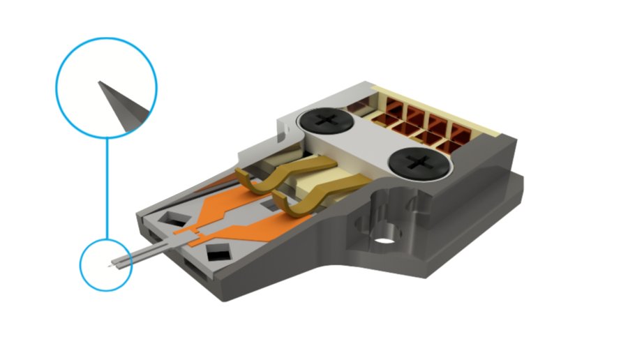
The go-to probe for CPEM measurements thanks to its visible tip. Capable of measuring AFM topography and energy dissipation signal at the same time. Measurement modes: Topography, Energy dissipation
CATEGORY
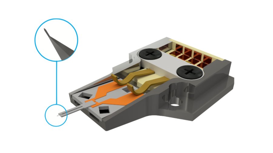
Magnetic-sensitive probe based on the Akiyama sensor, that can be used in SEM thanks to its visible tip. It uses the same probe holder as regular Akiyama. Measurement modes: Topography, MFM
CATEGORY