By MEMSIC Inc.
MXC3420AL 3-Axis Accelerometer MEMSIC MXC3420AL Datasheet V1.0 Page 1 of 53 2020/08 GENERAL DESCRIPTION The MXC3420AL is a small form factor, integrated digital output 3-axis accelerometer with a feature set optimized for industry applications, likes industry automatic control, device motion and tilt monitoring, remote controls, robot controls, etc. The MXC3420AL features a dedicated motion block which implements algorithms to support “any motion” and shake detection, tilt/flip and tilt 35 position detection. Low power consumption and small size are inherent in the monolithic fabrication approach, where the MEMS accelerometer is integrated in a single-chip with the electronics integrated circuit. In the MXC3420AL the internal sample rate can be set from 128 to 1024 samples / second. The device supports the reading of sample and event status via polling or interrupts. FEATURES Range, Sampling & Power • ±2, ± 4, ±8, ±12, ± 16g range • 16-bit resolution • 128 to 1024 Output Data Rate • 4 μA typical Standby current • Low typical active current Simple System Integration • I2C interface, up to 1 MHz • 2×2×0.92 mm 12-pin LGA package • High reliability thru single-chip 3D silicon MEMS technology • Mechanical Shock 20000G • RoHS compliant Applications • Industrial automatic control • Smart robot controls • Motion and tilt monitoring • Remote controls • Alarm module 1 ORDER INFORMATION Table 1. Order Information Table 2. Package Information Part Number Resolution Order Number Package Shipping MXC3420AL 16-bit MXC3420AL VLGA-12 Tape & Reel, 10Ku 2 FUNCTIONAL BLOCK DIAGRAM A/D Converter (Sigma Delta) C to V VPP VDD/VDDIO GND Regulators and Bias Oscillator/ Clock Generator Mode Logic I2C Slave Interface Interrupt XYZ OTP Memory Registers (64 x 8) SCL SDA INTN Offset/ Gain Adjust X,Y,Z data paths Sensors Range & Scale en Motion Block Figure 1. Block Diagram 3 PACKAGING AND PIN DESCRIPTION 3.1 PACKAGE OUTLINE 43b58962712 11 LL1 10 L1 e1 ASIDE VIEW BOTTOM VIEW 123410 9875 612 11 1PIN 1 MARK DIMENSION (MM) SYMBOL MIN. NOM. MAX. A 0.85 0.92 1.00 2.00 BSC 2.00 BSC 0.5 BSC e1 0.5125 REF b 0.20 0.25 0.30 L1 0.05 0.10 0.15 L 0.225 0.275 0.325 DEeE 0.10 0.10 DINDEX AREA 0.08 0.10 // TOP VIEW eL b 0.10 C 0.10 C Figure 2. Package Outline and Mechanical Dimensions 3.2 PACKAGE ORIENTATION Direction of Earth gravity acceleration XOUT = -1g YOUT = 0g ZOUT = 0g XOUT = +1g YOUT = 0g ZOUT = 0g XOUT = 0g YOUT = -1g ZOUT = 0g XOUT = 0g YOUT = +1g ZOUT = 0g XOUT = 0g YOUT = 0g ZOUT = +1g XOUT = 0g YOUT = 0g ZOUT = -1g Top View Side View Pin 1 Top a. b. c. d. e. f. Figure 3. Package Orientation -X +X +Y -Y +Z -Z Figure 4. Package Axis Reference 3.3 PIN DESCRIPTION Pin Name Function 1 VPP Connect to GND 2 SDA 1 I2C serial data input/output 3 VDD/VDDIO Power supply 4 NC No connect 5 INTN 2 Interrupt active LOW 3 6 NC No Connect 7 NC No Connect 8 NC No Connect 9 GND Ground 10 NC No Connect 11 NC No connect 12 SCL 1 I2C serial clock input Table 3. Pin Description Notes: 1) This pin requires a pull-up resistor, typically 4.7kΩ to pin VDD/VDDIO. Refer to I2C Specification for Fast-Mode devices. Higher resistance values can be used (typically done to reduce current leakage) but such applications are outside the scope of this datasheet. 2) This pin can be configured by software to operate either as an open-drain output or push-pull output ( mode register ). If set to open-drain, then it requires a pull-up resistor, typically 4.7kΩ to VDD/VDDIO. 3) INTN pin polarity is programmable in the mode register. 3.4 TYPICAL APPLICATION CIRCUITS To Fast-Mode I2C circuitry 1 Place cap close to VDD and GND on PCB } NOTE 1: Rp are typically 4.7kΩ pullup resistors to VDD/VDDIO, per I2C specification. When pin VDD/VDDIO is powered down, SDA and SCL will be driven low by internal ESD diodes. NOTE 2: Attach typical 4.7kΩ pullup resistor if INTN is defined as open-drain. VPP SDA VDD/VDDIO NC NC GND NC NC SCL NC INTN NC (optional) To MCU interrupt input 2 0.1μF 123410 9875 612 11 Rp Rp Rp Figure 5. Typical Application Circuit for 3DOF Solution In typical applications, the interface power supply may contain significant noise from external sources and other circuits which should be kept away from the sensor. Therefore, for some applications a lower-noise power supply might be desirable to power the VDD/VDDIO pin. 3.5 TAPE AND REEL Devices are shipped in reels, in standard cardboard box packaging. See Figure 6. MXC3420AL Tape Dimensions and Figure 7. MXC3420AL Reel Dimensions. • Dimensions in mm. • 10 sprocket hole pitch cumulative tolerance ± 0.2 • Pocket position relative to sprocket hole measured as true position of pocket, not pocket hole. Figure 6. MXC3420AL Tape Dimensions • Dimensions in mm. Figure 7. MXC3420AL Reel Dimensions 3.6 SOLDERING PROFILE The LGA package follows the reflow soldering classification profiles described in Joint Industry Standard, Moisture/Reflow Sensitivity Classification for Nonhermetic Surface Mount Devices,document number J-STD-020E. Reflow soldering has a peak temperature (T p) of 260 ⁰C 3.7 SHIPPING AND HANDLING GUIDELINES Shipping and handling follow the standards described in Joint Industry Standard, Handling, Packing, Shipping and Use of Moisture/Reflow Sensitive Surface Mount Devices, document number J-STD-033C. The following are additional handling guidelines (refer to the MEMSIC document, PCB Design, Device Handling and Assembly Guidelines, for more information): • While the mechanical sensor is designed to handle high-g shock events, direct mechanical shock to the package should be avoided. • SMT assembly houses should use automated assembly equipment with either plastic nozzles or nozzles with compliant tips (for example, soft rubber or silicone). • Avoid g-forces beyond the specified limits during transportation. • Handling and mounting of sensors should be done in a defined and qualified installation. 3.8 MOISTURE SENSITIVITY LEVEL CONTROL The following are storage recommendations (refer to the MEMSIC document, PCB Design, Device Handling and Assembly Guidelines, for more information): • Store the tape and reel in the unopened dry pack, until required on the assembly floor. • If the dry pack has been opened or the reel has been removed from the dry pack, reseal the reel inside of the dry pack with a black protective belt. Avoid crushing the tape and reel. • Store the cardboard box in a vertical position. 4 SPECIFICATIONS 4.1 ABSOLUTE MAXIMUM RATINGS Parameters exceeding the Absolute Maximum Ratings may permanently damage the device. Rating Symbol Minimum / Maximum Value Unit Supply Voltages Pin VDD/VDDIO -0.3 / +3.6 V Acceleration, any axis, 200 μs g MAX 20000 g Ambient operating temperature TOP -40 / +105 ⁰C Storage temperature TSTG -40 / +150 ⁰C ESD human body model HBM ± 4000 V Latch-up current at T op = 25 ⁰C ILU 200 mA Input voltage to non-power pin Pins INTN, SCL and SDA -0.3 / (VDD + 0.3) or 3.6 whichever is lower V Table 4. Absolute Maximum Ratings 4.2 SENSOR CHARACTERISTICS VDD = 2.8V, T op = 25 ⁰C unless otherwise noted Parameter Conditions Min Typ Max Unit Acceleration range ±2.0 ±4.0 ±8.0 ±12.0 ±16.0 g Sensitivity Acceleration range = ±2.0g 16384 LSB/g Acceleration range = ±4.0g 8192 Acceleration range = ±8.0g 4096 Acceleration range = ±12.0g 2730 Acceleration range = ±16.0g 2048 Sensitivity Temperature Coefficient 1 -40 ≤ T op ≤ +85 ⁰C ±0.015 %/ ⁰C Zero-g Offset Chip Level Board Level ±20 ±50 mg Zero-g Offset Temperature Coefficient 1 -40 ≤ T op ≤ +85 ⁰C ±0.5 mg/ ⁰C RMS Noise ODR = 1024 0.8 (X,Y) 1.5 (Z) mg RMS Nonlinearity 1 Acceleration range = ±2.0g 0.4 % FS Cross-axis Sensitivity 1 Between any two axes ±1 % ODR, Output Data Rate 128 1024 Hz 1 Values are based on device characterization, not tested in production. Table 5. Sensor Characteristics 4.3 ELECTRICAL AND TIMING CHARACTERISTICS 4.3.1 ELECTRICAL POWER AND INTERNAL CHARACTERISTICS Parameter Conditions Symbol Min Typ Max Unit Supply voltage 1 Pin VDD/VDDIO VDD 1.7 3.6 V Sample Rate Tolerance 2 Tclock -2 2 % 1 Min and Max limits are hard limits without additional tolerance. 2 Values are based on device characterization, not tested in production. Test condition: VDD = 2.8V, T op = 25 ⁰C unless otherwise noted Parameter Conditions Min Typ Max Unit Standby current 4 μA WAKE state current ODR = 128 Hz 73 μA Pad Leakage Per I/O pad -1 0.01 1 μA Wake-Up time 3 ms Start-Up time 1/ODR+1mS ms Table 6. Electrical Characteristics 4.3.2 I2C ELECTRICAL CHARACTERISTICS Parameter Symbol Min Max Unit LOW level input voltage VIL -0.5 0.3*VDD V HIGH level input voltage VIH 0.7*VDD - V Hysteresis of Schmitt trigger inputs Vhys 0.05*VDD - V Output voltage, pin INTN, Iol ≤ 2 mA Vol Voh 0 0 0.4 0.9*VDD V V Output voltage, pin SDA (open drain), Iol ≤ 1 mA Vols - 0.1*VDD V Input current, pins SDA and SCL (input voltage between 0.1*VDD and 0.9*VDD max) Ii -10 10 μA Capacitance, pins SDA and SCL 1 Ci - 10 pF 1 Values are based on device characterization, not tested in production. Table 7. I2C Electrical and Timing Characteristics NOTES: • If multiple slaves are connected to the I2C signals in addition to this device, only 1 pull-up resistor on each of SDA and SCL should exist. Also, care must be taken to not violate the I2C specification for capacitive loading. • When pin VDD/VDDIO is not powered and set to 0V, INTN, SDA and SCL will be held to VDD plus the forward voltage of the internal static protection diodes, typically about 0.6V. • When pin VDD/VDDIO is disconnected from power or ground (e.g. Hi-Z), the device may become inadvertently powered up through the ESD diodes present on other powered signals. 4.3.3 I2C TIMING CHARACTERISTICS Figure 8. I2C Interface Timing Parameter Description Standard Mode Fast Mode Fast Mode Plus Units Min Max Min Max Min Max fSCL SCL clock frequency 0 100 0 400 0 1000 kHz tHD; STA Hold time (repeated) START condition 4.0 - 0.6 - 0.26 - μs tLOW LOW period of the SCL clock 4.7 - 1.3 - 0.5 - μs tHIGH HIGH period of the SCL clock 4.0 - 0.6 - 0.26 - μs tSU;STA Set-up time for a
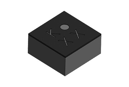
WLP package, 0.85x0.85x0.4mm, I²C/I³C interface, ±30g range, high performance AMR Magnetometer Application: Smart Phone/Pad/NoteBook; Wearable Device; Smart Home; Smart Device Monolithic integrated 3-axis AMR magnetic sensor and electronic circuits requiring fewer external components Superior Dynamic Range and Accuracy ±30 G FSR 20bits operation mode 0.0625mG per LSB resolutio 2 mG total RMS noise Enables heading accuracy of ±1º Sensor true frequency response up to 1KHz Ultra-Small Wafer Level Package 0.8x0.8x0.4mm On-chip automatic degaussing with built-in SET/RESET function Eliminates thermal variation induced offset error (Null field output) Clears the residual magnetization resulting from strong external fields On-chip sensitivity compensation On-chip temperature sensor Selftest signal available Dataready Interrupt (I³C only) Low power consumption 1µA power down current I²C slave, FAST (≤400 KHz) mode I³C interface, Compatible with MIPI I³C pecfication version 1.0 1.62V to 3.6V wide range single power supply 1.2V compatible I²C interface 1.8V 1.8V compatible I³C interface RoHS complian
CATEGORY
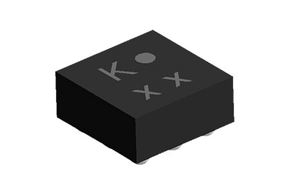
BGA package, 1.2x1.2x0.5mm, I²C interface, ±30g range, high performance AMR Magnetometer Application: Wearable Device, Smart Home, Smart Device Fully integrated 3-axis magnetic sensor and electronic circuits requiring fewer external components Superior Dynamic Range and Accuracy ±30G FSR with 16bits operation 1mG per LSB resolution 2mG total RMS noise Enables heading accuracy of 1º Output data rate up to 600 Hz Ultra Small Low profile package 1.2x1.2x0.5mm Degaussing with built-in SET/RESET function Eliminates thermal variation induced offset error (Null field output) Clears the residual magnetization resulting from strong external fields On-chip sensitivity compensation On-chip temperature sensor MotionDetection and DataReady Interrupt Low power consumption 1µA power down current I²C Slave, FAST (≤400 KHz) mode 1.8V single low power supply compatible Low to 1.2V I²C interface RoHS compliant
CATEGORY
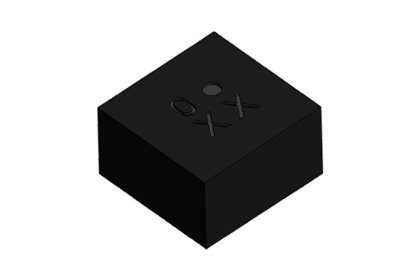
BGA package, 1.6x1.6x0.6mm, multiple I²C device addresses, I²C interface, ±16g range, high performance AMR Magnetometer Fully integrated 3-axis magnetic sensor and electronic circuits requiring fewer external components Superior Dynamic Range and Accuracy ±16G FSR with 16/14bits operation 0.5mG/2mG per LSB resolution in 16/14bits operation mode 1.5mG total RMS noise Enables heading accuracy of ±1º Max output data rate of 800 Hz (12 bits mode) Ultra Small Low profile package 1.6x1.6x0.6mm Allows for elimination of temperature variation induced offset error (Null field output) Clears the sensors of residual magnetization resulting from strong external fields On-chip sensitivity compensation Low power consumption (140µA @ 7Hz ) 1µA (max) power down function I²C Slave, FAST (≤400 KHz) mode 1.62~3.6V wide power supply operation supported, 1.8 V I/O compatibility RoHS compliant
CATEGORY
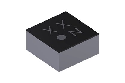
WLP package, 0.8x0.8x0.4mm, I²C interface, ±30g range, high performance AMR Magnetometer Monolithic integrated 3-axis AMR magnetic sensor and electronic circuits requiring fewer external components Superior Dynamic Range and Accuracy ±30G FSR 20bits operation mode 0.0625mG per LSB resolution 2mG total RMS noise Enables heading accuracy of 1º Sensor true frequency response up to 1KHz Ultra-Small Wafer Level Package 0.8x0.8x0.4mm On-chip automatic degaussing with built-in SET/RESET function Eliminates thermal variation induced offset error (Null field output) Clears the residual magnetization resulting from strong external fields On-chip sensitivity compensation On-chip temperature sensor Selftest signal available Low power consumption 1µA power down current I²C slave, FAST (≤400 KHz) mode 1.62V to 3.6V wide range single power supply 1.2V logic IO RoHS compliant
CATEGORY
