Plus Custom Semiconductor, Metal and Oxide Nanomaterial Designs - Driven by Application Requirements.
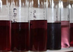
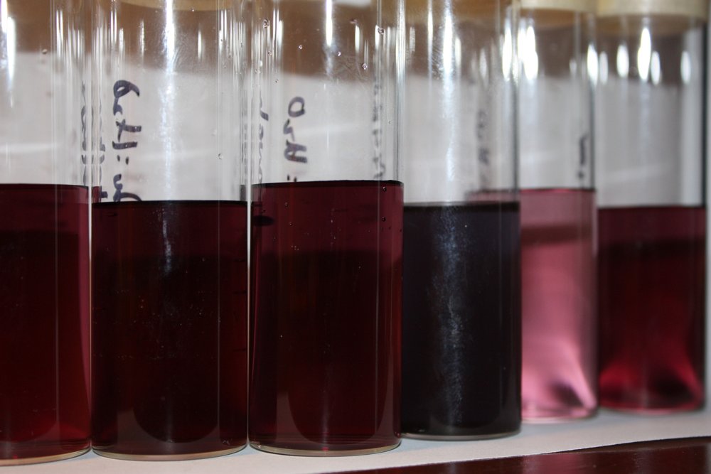
Gold nanoparticles are a versitile material whose natural resistance to surface oxidation makes it ideal for a wide-range of electronic and photonic applications. Gold nanoparticles can range in color from red to purple depending on the particle size. Nano sized gold finds wide-ranging applications, when leveraging their characteristically high surface-to-volume ratio. Dispersions of gold nanoparticles are designed in collaboration with the customer, based on their application-specific needs, with mean particle diameters ranging from 1nm to 100 nm. Designs of gold nanoparticles encompass two generic product spaces: aqueous stabilized dispersion, and organic stabilized dispersion. Custom form factors and solvents are available upon request. Both the sample size of gold nanoparticles, and concentration may be designed as required, to concentrations as high as 50 volume percent (a paste form). Aggregate Surface Area, gold nanoparticles: - 38 sq. meters/gram (8 nm material) - 24 sq. meters/gram (13 nm material) - 18 sq. meters/gram (17 nm material) Meliorum Technologies has spent the past ten years perfecting its proprietary technology for formulating gold nanoparticles with defined features. Hundreds of instances of these formulations are featured in high impact academic journals worldwide. Gold nanoparticles can be formulated in a particularly wide variety of waterbourne and organic liquid solvents. The choice is yours, and it is driven by your research needs and/or application requirements. FIGURE 1 Gold nanoparticles in various sizes and concentrations FIGURE 2 Black Graph - Approx. 8 nm size Gold nanoparticles; Red Graph - Approx. 13 nm size Gold nanoparticles; Blue Graph - Approx. 17 nm size Gold nanoparticles (Measurements taken via photon correlation spectroscopy light scattering analysis)
CATEGORY
Silicon (Si) nanoparticles are an exciting and relatively versatile material which will revolutionize the electro-optic semiconductor industry. Meliorum silicon nanoparticles are available in powder form, as well as dispersion formulations in standard and custom solvents. TEM Image, 30 nm mean diameter Black Graph - 5nm size distribution,Silicon nanoparticle s Red Graph - 30 nm size distribution,Silicon nanoparticles (Measurements taken via photon correlation spectroscopy light scattering analysis) Bulk silicon is an indirect band gap semiconductor, which means it is a highly inefficient source of light. However, silicon nanoparticles (as small as ~5 nm in diameter) have been demonstrated as an efficient visible light source. In fact, even single silicon nanoparticles can be seen with little complex instrumentation, given the appropriately engineered silicon nanoparticle surface chemistry. Silicon nanoparticles find potential applications in solid state lighting, lasers, microelectronics, biological tags, etc. It is non-toxic to the human body, in contrast to other semiconductor materials. Silicon nanoparticles are a spectrally broad photoluminescent product, but may be tuned thoughout the visible spectrum with additional silicon nanoparticle post-processing steps, based on your application needs. This will be discussed on a collaborative basis, or Meliorum will refer customers to various publications to outline appropriate processing techniques. Products of silicon nanoparticles may be designed in two primary size distribution choices: 30 nm or 5 nm. Other sizes available on a custom basis. Aggregate Surface Area, Silicon nanoparticles: - 86 sq. meters/gram (30 nm silicon nanoparticles) - 644 sq. meters/gram (5 nm silicon nanoparticles)
CATEGORY
Ceria (cerium oxide, CeO 2) nano abrasive powder finds applications in the precision polishing of most semiconductor substrate materials including silicon, sapphire, GaAs, etc. Ceria nano abrasive powder has been shown to not only demonstrate tremendous advantages in the planarization process of most semiconductor materials but glassy materials employed in photonic applications as well. Ceria powder is designed based on application-specific needs as stated by the customer, in scaled quantities with a mean particle diameter of 8 nm. It can be designed in various form factors: powder, aqueous pH modified dispersion, and organic liquid dispersion. Custom form factors are available upon request. Red Graph - Particle Size Distribution Black Graph - Cumulative Size Distribution (Measurements taken via photon correlation spectroscopy light scattering analysis) Meliorum NanoCeria PDF Datasheet: Both the sample size and concentration may be designed as required, to concentrations as high as 50 volume percent (a paste form). Nanoparticle Aggregate Surface Area: - 44 sq. meters/gram Cerium Oxide research quantity packaging
CATEGORY
Formulated over ten years ago, "ink" dispersions of silicon nanoparticles are a specially formulated dispersion usable for printing applications. The silicon nanoparticles feature a proprietary and customizable surface functionalization that enhances its ability to be incorporated in thin film deposition, layer sintering, and other related industrial and research applications. Custom surface functionalization of silicon nanoparticles can be made to be compatible with polar or nonpolar carrier solvents, as needed. Additionally, the silicon nanoparticles may be provided with custom dopants and concentrations, for semiconductor materials research.
CATEGORY
