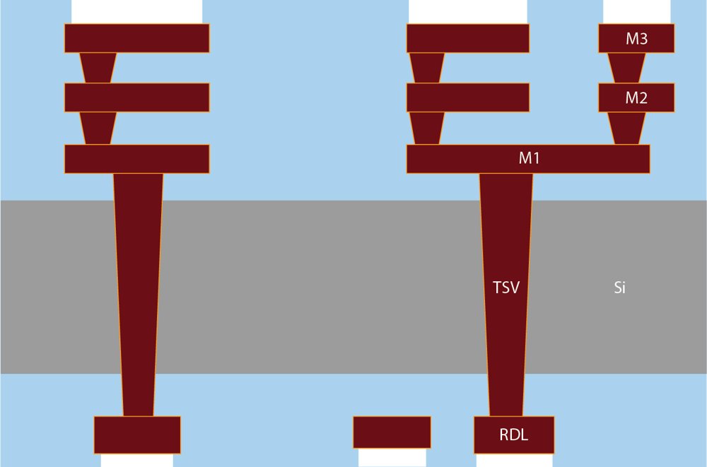
The electronic interposer is a silicon (Si) wafer used for enabling 2.5D integration of photonic and electronic integrated circuits for advanced packaging. Copper (Cu) lines on the top surface are routed to a backside Cu redistribution layer (RDL) using 10 x 100 µm thru-silicon vias (TSVs). The terminal metal can be bumped (Cu pillar, C2, or C4 solder bumps) for flip-chip packaging. Advanced packaging operations, such as wafer bumping, flip-chip attach and board assembly, are supported through AIM Photonics Test, Assembly, and Packaging (TAP) facility. Design Information AIM Photonics has developed an Electronic Interposer PDK which is supported by the Analog Photonics Electronic Interposer and RF/SUNY Electronic Interposer component libraries. Design rule check is supported in Cadence PVS, Synopsys ICV, and KLayout. Customization While we typically follow a standard process flow that designers cannot modify, AIM Photonics has developed a “bite-size” custom offering in which designers can make minor changes to the process flow for an additional fee. This is not a full custom run, and the modification must be something the fab team can execute without additional development work. The exact specifications and complexity of the design may affect which run it will ultimately ride on, and in most cases, this can vary between one and two months. Please contact us well in advance of the design due date to ensure that our team understands your request and can properly quote the work. Customization Options Currently Available for Electronic Interposers - Aluminum termination Schedule Year | Run ID | Design Due Date | Expected Ship Date 2025 | EI 25-04E | Dec 3, 2025 | Mar 3, 2026 2026 | EI 26-01E | Mar 2, 2026 | Jun 1, 2026 EI 26-02E | Jun 1, 2026 | Sep 1, 2026 EI 26-03E | Sep 1, 2026 | Dec 1, 2026 EI 26-04E | Dec 1, 2026 | Mar 2, 2027 Pricing Electronic Interposer | Member (per 20 qty chips) | Non-Member (per 20 qty chips) 156 mm 2 | $90,000 | $108,000
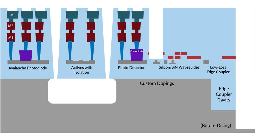
The MPW QFlex PIC consists of one silicon, two ridge, and two silicon nitride waveguides. Twelve implant levels are available for active component design, a Ge photodetector, Avalanche Photodetector, two copper wiring levels, and an aluminum termination with passivation oxide and a pad opening. The standard offering has a trench with substrate release, a separate extrinsic material cavity trench and a low-loss edge coupler to eliminate substrate absorption. On the base active build, the silicon (SE) waveguide propagation loss target is 0.40 dB/cm and Rib (RE) target is ~ 0.150 dB/cm, while the silicon nitride waveguide propagation loss target is 0.10 dB/cm. Current Silicon Nitride on the fully Integrated build is 0.325 db/cm (at 1550 nm. No delta exists between 1520 nm and 1550 nm. Future offering demonstrated SIN < 0.1 db/cm (1550 nm) on a full active run. Design Information The QFlex PIC is supported by the component library from the Research Foundation for SUNY (RFS): - The RFS library is a comprehensive, high-performance, open and black box library focused on wavelength operations in the O, C, and L bands. Schedule Year: 2026 | Run ID: QFlex 26-03Q | Design Due Date: Aug 15, 2026 | Expected Ship Date: Mar 15, 2027 Pricing (per 20 qty chips) - 8 mm2: Member $45,000 | Non-Member $54,000 - 25 mm2: Member $90,000 | Non-Member $108,000 - 50 mm2: Member $180,000 | Non-Member $216,000 - 100 mm2: Member $360,000 | Non-Member $432,000 Notes - Start dates for runs are subject to change. - Member prices shown are for customers who are Full Active Members and have executed an AIM Photonics Membership Agreement. - Customer receives 20 qty unpackaged chips of the size/technology ordered. - All chips are placed in a gel-pack and shipped to the customer as part of Standard MPW Offerings pricing. - For an additional charge, sub-dicing or post processing is available – please see information about Testing, Assembly and Packaging (TAP) Services. - All pricing shown subject to change
CATEGORY
Interposer wafers offer the ability to combine the advantages of photonic and electronic components to enable complex, compact and energy-efficient photonic integrated circuits (PICs). We use advanced waveguide fabrication methods that improve silicon waveguide propagation loss to < 0.5 dB/cm while the silicon nitride waveguide propagation loss is < 0.35 dB/cm.
CATEGORY
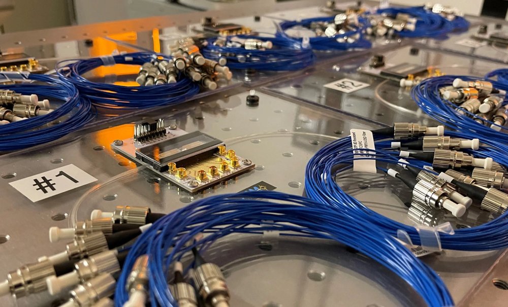
a six-chip photonic integrated chip (PIC) kit focused on the fundamental concepts used in data communications, including: - Insertion Loss - Interference - Mach-Zehnder Modulation - Germanium Photodetectors - Ring Resonator – Wavelength Division Multiplexing (WDM) / Demultiplexing - WDM Micro-ring Modulation
CATEGORY
