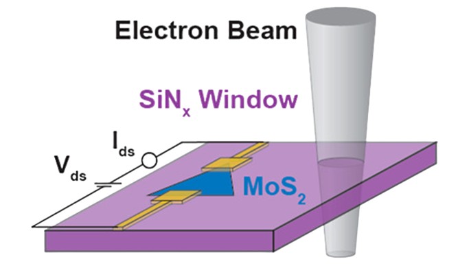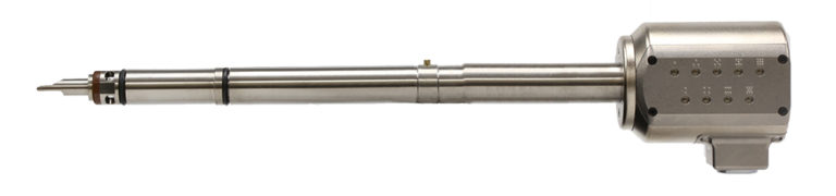
The Hummingbird Scientific TEM MEMS Heating + Biasing Sample Holder enables simultaneous high-temperature heating and electrical biasing during in-situ TEM and STEM experiments. Designed for researchers in semiconductor devices, energy storage, catalysis, materials science, nanotechnology, and electronics, it supports investigations of phase transformations, electrical transport, electromigration, nanoscale diffusion, device failure, battery cycling, and catalyst activation. By directly correlating thermal and electrical stimuli with surface morphology, chemical composition, and electrical response, researchers can reveal the mechanisms governing material performance and degradation under realistic operating conditions. Hummingbird Advantages: - Screw-free direct MEMS chip insertion for fast, reproducible sample loading. - Closed-loop MEMS heating from room temperature to above 1000 °C with integrated temperature sensing. - Nine direct-chip electrical contacts for simultaneous electrical biasing and electrical measurements. - Full compatibility with TEM, STEM, EDS, and EELS during heating and biasing experiments. - Available in single-tilt and high-accuracy double-tilt configurations for optimal sample orientation. - Supports diverse experiments with FIB lift-out chips, multiple chip electrode materials and geometries, and custom MEMS chip designs. - Compatible with TEM, SEM, and X-ray microscopy workflows using cross-platform microfabricated chips. How it Works: The TEM MEMS Heating + Biasing Sample Holder combines Hummingbird Scientific's in-house microfabricated MEMS chips, direct electrical contacts, and closed-loop temperature control to create a stable platform for simultaneous in-situ heating and electrical biasing inside the TEM. Samples are mounted directly onto a MEMS chip and inserted into the holder using a screw-free loading mechanism, enabling fast, reproducible experiment setup. During operation, the MEMS microheater delivers temperatures up to above 1000 °C, while on-chip 4-point resistance sensing enables closed-loop temperature control for stable real-time imaging and analysis. Heating + Biasing MEMS chips support simultaneous thermal and electrical stimulation, while biasing MEMS chips dedicate all nine contacts to electrical measurements when heating is not required. The double-tilt configuration adds high-accuracy beta tilt controlled by dedicated tilting software, enabling precise sample orientation for diffraction, crystallographic, and analytical in-situ TEM experiments. Key Features and Capabilities: Screw-Free Direct Chip Insertion: Load MEMS chips directly into the holder using a screw-free insertion mechanism with spring-loaded electrical contacts. Eliminate delicate alignment, wire bonding, and complex mounting procedures while establishing consistent electrical contact. This simplified loading process reduces setup time, improves experiment reproducibility, and enables rapid sample exchange between experiments. Benefits: Minimize experiment setup time; Improve electrical contact reliability and experiment repeatability; Simplify MEMS chip exchange; Eliminate handling of small screws and manual alignment of electrical contacts. Nine Low-Noise Electrical Contacts: Advanced electrical characterization requires stable, low-noise signal transmission throughout the experiment. Individually shielded coaxial cabling inside and out of the holder and nine direct-chip electrical contacts minimize electrical interference while supporting simultaneous heating, electrical biasing, multi-terminal measurements, and independent sample grounding for greater experimental flexibility. Benefits: Exceptional flexibility for simultaneous heating, electrical biasing, grounding, and multi-terminal device characterization; Minimized electrical noise for stable, high-fidelity electrical measurements; Simultaneous heating and electrical biasing without sacrificing measurement capability; Increase experimental versatility for semiconductors, batteries, and nanoelectronic devices. Closed-Loop MEMS Heating Above 1000 °C: Microfabricated MEMS microheaters deliver temperatures above 1000 °C, while integrated on-chip 4-point resistance sensing enables accurate closed-loop temperature control. Localized heating minimizes thermal loading of the holder and microscope, supporting stable imaging and long-duration experiments. With up to 9 biasing contacts, biasing experiments can be performed concurrently with heating to correlate multiple properties and applied conditions to observed transformations. Benefits: Heat samples above 1000 °C to study high-temperature material transformations; Achieve rapid temperature cycling for dynamic in-situ TEM heating experiments; Reliably heat samples with stable temperatures applied over long-duration in-situ TEM experiments; Minimize heat transfer to the substrate for improved image stability and microscope safety; Near-drift-free operation throughout the temperature range during high-resolution imaging. High-Accuracy and Repeatable Double Tilt: The high-accuracy double-tilt configuration adds a precision beta tilt axis with minimal backlash, enabling accurate, repeatable sample orientation for demanding in-situ TEM experiments and precise imaging conditions. Independent alpha and beta tilt provide greater flexibility for diffraction, crystallographic analysis, high-resolution and atomic resolution imaging, and analytical TEM workflows where precise sample alignment is essential. Benefits: Optimize sample orientation for in-situ crystallographic and diffraction experiments; Support high-resolution imaging by achieving optimal specimen alignment; Align crystalline samples precisely for orientation-sensitive experiments; Enhance reproducibility across repeated tilt-dependent experiments. Multimodal Characterization: Our MEMS heating and electrical biasing platform extends beyond TEM with compatible holders for SEM and synchrotron X-ray microscopy platforms, enabling seamless correlative in-situ characterization across multiple length scales using the same MEMS chips. This integrated workflow combines simultaneous thermal and electrical stimulation with complementary imaging and spectroscopy, providing a more complete understanding of temperature- and electrically driven nanoscale material behavior under realistic operating conditions. Benefits: Use the same MEMS chips across TEM, SEM, and X-ray microscopy platforms; Generate cross-correlative imaging and spectroscopic datasets across length scales; Overcome the limitations of individual microscopy and spectroscopy techniques. 60+ In-Stock TEM Heating and Biasing Chip Configurations: Hummingbird Scientific microfabricates MEMS chips in-house and maintains standard Heating, Electrical Biasing, Heating + Biasing, and FIB lift-out configurations in stock for rapid delivery. Quality-controlled chips are clean packed and ready to use out of the box, with a broad selection of heater designs, electrode layouts, materials, and window geometries. The same MEMS chip platform is compatible across Hummingbird's TEM, SEM, and synchrotron X-ray heating and biasing systems, while custom MEMS chip designs support specialized applications and experimental workflows. Benefits: 60+ standard TEM heating and biasing chip configurations in stock; Easy online ordering and 24-hour shipping to keep in-situ experiments moving; Cross-platform chips compatible across our TEM, SEM, and X-ray heating + biasing sample holders; Made-to-order custom chips for specialized heating and biasing TEM experiments also available. High-Voltage Biasing (optional add-on feature): Augment the TEM MEMS Heating + Biasing Sample Holder for specialized high-voltage electrical biasing up to 1 kV. Optimized cabling, electrical interfaces, and sample carrier configurations maintain stable electrical performance while supporting simultaneous MEMS heating and in-situ TEM imaging. This capability enables researchers to investigate high-electric-field phenomena, dielectric breakdown, electrical switching, device reliability, and failure mechanisms under realistic operating conditions. Benefits: Supports simultaneous heating and high-voltage biasing within a single in-situ TEM experiment; Maintains stable electrical performance with optimized high-voltage hardware and cabling; Helps investigate dielectric breakdown, electrical switching, and device failure mechanisms in-situ.