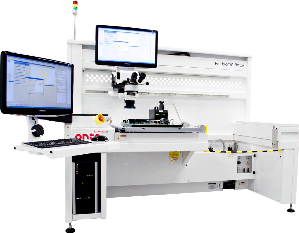
The PrecisionWoRx VX4 System is designed to provide accurate and repeatable performance through enhanced testing of the latest probe card technologies with tighter pitches, smaller pads and higher pin counts. The PrecisionWoRx VX4 System gives test facilities and probe card manufacturers the ability to confidently test tighter pitches and smaller probe tips. The system can be configured to meet specific requirements for a variety of probe card technologies. For processes using cards with very small probe tips, the system’s high-resolution optics deliver a detailed field-of-view for high accuracy and repeatability. Proprietary image-processing recipes control over 30 imaging parameters for enhanced testing of most probe tip geometries in use today. The PrecisionWoRx VX4 System improves overall cost of ownership with faster test times for common tests, including leakage, planarity, alignment, contact resistance, probe force and wire checker. Its sophisticated electrical discharge management capability maintains 1-volt continuity to the probe during electrical testing. Productivity-enhanced routines for automated testing of failed probes and a wide variety of checkplates suit an extensive range of process and technology requirements. The system provides support for the most complex probe card technologies. Applications - Various probe tips from 5 µm up to 250 µm diameter - Z force up to 200 KG - Pin counts >100,000 probes - Direct dock probe card capabilities - Probe card relay and solid-state switching - Membrane probe cards
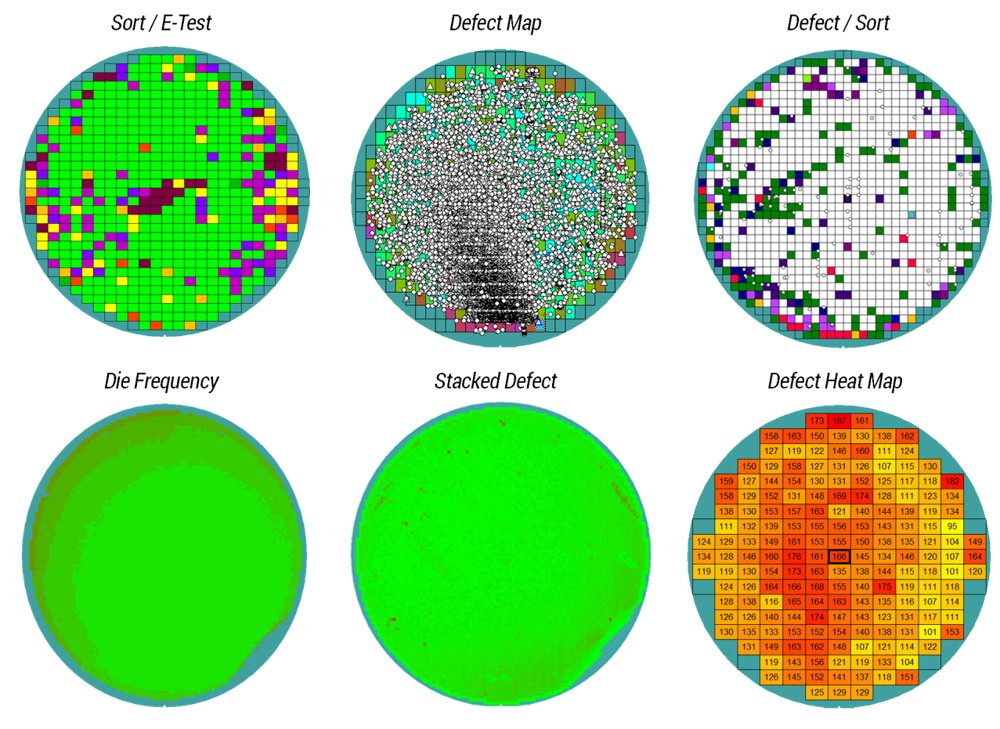
Comprehensive mapping suite that covers all aspects of semiconductor processes
CATEGORY
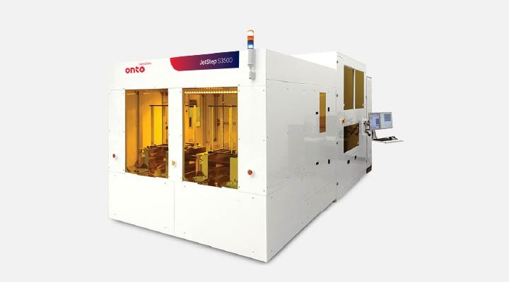
An advanced feed-forward lithography software solution for fan-out panel level packaging that enhances yield and throughput by correcting die placement errors through external measurements, predictive analytics and adaptive shot control. StepFAST® software is Onto Innovation’s advanced lithography software solution tailored for fan-out panel-level packaging, where die placement errors and material instability can significantly impact yield and productivity. StepFAST® software uses a feed-forward adaptive shot approach, integrating high-speed die placement measurements from the Firefly® system and applying real-time corrections to every shot of the JetStep® lithography tool. This external measurement strategy doubles throughput compared to traditional on-tool (self-metrology) methods. The software also incorporates predictive yield analysis, enabling dynamic adjustment of exposure field sizes to balance throughput and overlay accuracy. By automating reticle selection and optimizing field coverage, StepFAST® software ensures efficient panel exposure while minimizing registration errors—from ±50µm down to under ±3µm. With advanced analytics, StepFAST® software transforms lithography into a flexible, high-efficiency process, delivering substantial improvements in yield, throughput, and cost of ownership for panel-level packaging applications. Applications: - Panel-level packaging Featured Markets: - Advanced Packaging Adaptive Shot Lithography Solution: Die shift on reconstituted panels can significantly impact both productivity and yield. To address this challenge, we use a parallel die placement measurement process and advanced analytics to provide a means to balance productivity against yield. Our integrated lithography cell, featuring Firefly inspection, StepFAST software, and JetStep Lithography, delivers industry-leading throughput and yield for fan-out panel level packaging.
CATEGORY
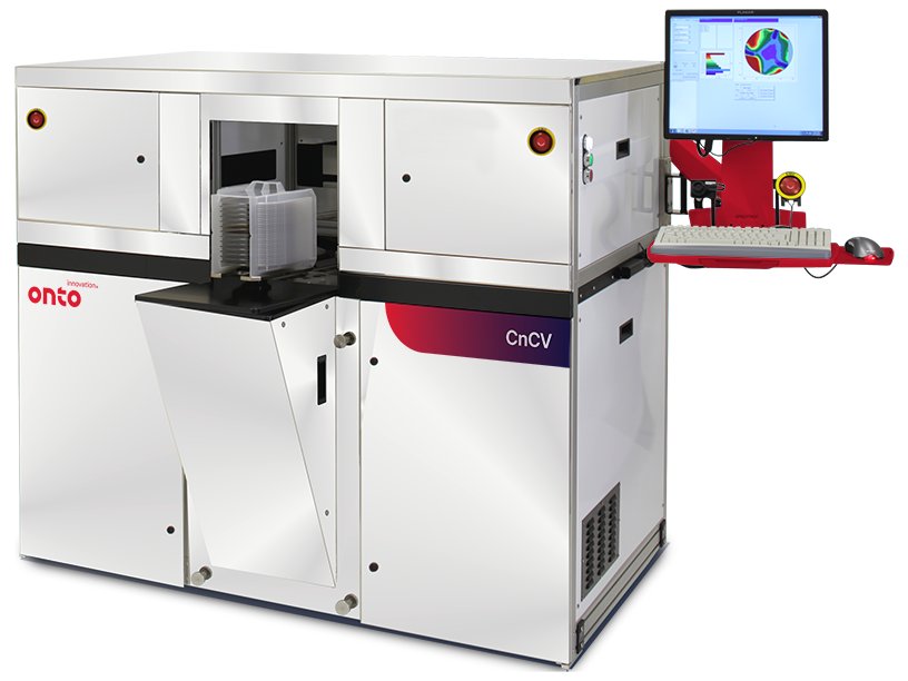
The CnCV system enables wafer-level characterization of WBG materials without test device fabrication, reducing time and cost. As a mercury-free alternative to MCV, it eliminates contamination concerns. The enhanced Kinetic CV mode with UV-assisted corona charge neutralization achieves high throughput and precision for fast, reliable process control. The CnCV system utilizes a novel constant surface potential corona charging, which enables the precision required over a large voltage range.The patented technology includes charge- and photo-assisted modes, especially suited for speed and precision on WBG materials and structures, including SiC,Ga 2 O 3, GaN, and AlGaN/GaN HEMT. Additionally, Corona-Kelvin characterization includes electrical properties of dielectrics and interfaces of films on SiC and GaN epi layers. An automated top-side edge contact (TSEC) is also available enabling characterization of WBG on insulating/semi-insulating substrates. Automated bias-temperature stress (BTS) measurements are also available with the CnCV system, providing a fast, noncontact way to quantify the reliability of passivated SiC and GaN. Beyond typical CV type parameters, the full wafer corona approach allows for QUAD (quality, uniformity, and defect) mapping. The electrical defect imaging, QUAD-EDI, mode is especially designed for SiC. It provides a unique means for quick screening of epi electrical defectivity enabling improvement in device yield prediction. Applications: - Non-contact epi dopant depth profiling in WBG materials - AlGaN\GaN HEMT measurements (pinch off voltage & 2DEG sheet charge) - Dielectric and interface characterization electrical defect imaging in SiC for yield prediction - Bias-temperature stress (BTS) instability measurements on passivated WBG materials Featured Markets: - Bare Wafer & Panel Manufacturing - Specialty
CATEGORY
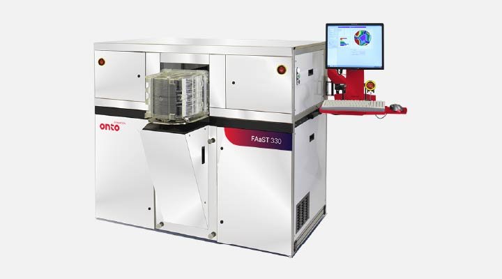
The FAaST system is a versatile, non-contact electrical metrology platform, with an option to combine micro and macro corona-Kelvin technologies together with digital surface photovoltage (SPV). It enables high-resolution dielectric and interface measurements across a wide range of dielectric materials, supporting both R&D and high volume manufacturing. The primary application of non-contact CV metrology is monitoring dielectric properties during IC manufacturing. Unlike conventional electrical measurements, it requires no sample preparation, eliminating the need for MOS capacitor structures. This reduces metrology cost and enables fast data feedback in both R&D and manufacturing environments. The corona-Kelvin method uses a corona discharge in air to deposit an electric charge (D Q C) on the wafer surface. A vibrating Kelvin-probe then measures the resulting surface voltage (V), enabling determination of the differential capacitance (C=D Q C/D V). By monitoring surface voltage in both dark and illuminated conditions, the system separates two key components: dielectric voltage (V D) and semiconductor surface potential (V SB), enabling determination of flat band voltage (V FB). Analysis of the resulting charge-voltage data yields electrical parameters, including trap density (D it), flat band voltage (V fb), dielectric charge (Q tot), dielectric capacitance (C D), Equivalent Oxide Thickness (EOT), leakage current, and tunneling characteristics. Applications - Plasma damage monitoring - Residual charge and non-visual defect inspection - Diffusion furnace oxide and interface characterization - High-K and low-K dielectric capacitance - Mobile ion mapping - Charge trapping and hysteresis Featured Markets - Bare Wafer & Panel Manufacturing - CMOS Technologies - Specialty - Advanced Packaging
CATEGORY
