The Ambient-pressure Photoemission Spectroscopy (APS) systems are one of KP Technology Ltd's most recent additions to our large surface analysis range. Domestic and international patents are held for these instruments. APS measures the absolute work function (Φ) of a material by photoemission in ambient conditions, no vacuum is required. The excitation range of APS is 3.4 eV to 7.0 eV, meaning that APS is capable of measuring the absolute work function of metals and the ionisation potential of semiconductors alongside measurement of the surface Fermi level with the Kelvin probe. If an SPV and SPS source is added to the APS system, the full bands of semiconductors can be measured in one complete desktop system; no other product in the world can do this. APPLICATIONS - Organic and non-organic semiconductors - Metals and metal alloys - Thin films and surface oxides - Solar cells and organic photovoltaics - Corrosion and nanotechnology FEATURES - Work function by photoemission in air - Density of states measurements - 3.4 eV to 7.0 eV energy range - Measurement of all semiconductor bands - Contact potential difference by Kelvin Probe SYSTEM OVERVIEW The optical enclosure houses the sample in complete darkness prior to measurement. The photoelectron detector measures the liberated electrons driven off by the UV light emitted by the monochromator. The UV bulb is powered by an external PSU and is controlled by software. The UV light is injected into the monochromator and a variable wavelength of light is produced. The energy range of this light is 3.4 eV to 7.0 eV. The digital controller controls every aspect of the system and is controlled by the dedicated software GUI. The measurement from the photoelectron detector is passed to the digital controller, to the PC and plotted in software, producing the PE curve. Kelvin probe 3-axis scanning Surface Photovoltage Tip material / diameter Au/Al, Silicon Solar Cell and Ag Reference samples CPD resolution 1 - 3 meV APS Measurement Resolution 0.05eV Height control (auto) 25 mm automatic Kelvin probe mode and PE mode CPD and photoemission measurements CPD measurement time CPD measurements in <1 minute WF measurement time PE measurements in <5 minutes Optical system Colour camera with zoom and monitor for positioning Oscilloscope Digital TFT oscilloscope for real time signal Test sample Au/Al, Silicon Solar Cell and Ag Reference samples Faraday/optical enclosure LE450 (450 mm x 450 mm) Control supplied PC control with dedicated software Patented technology US:8866505 / GB:2439439 / GB:2495998 / EU:2783205 / JP:6018645
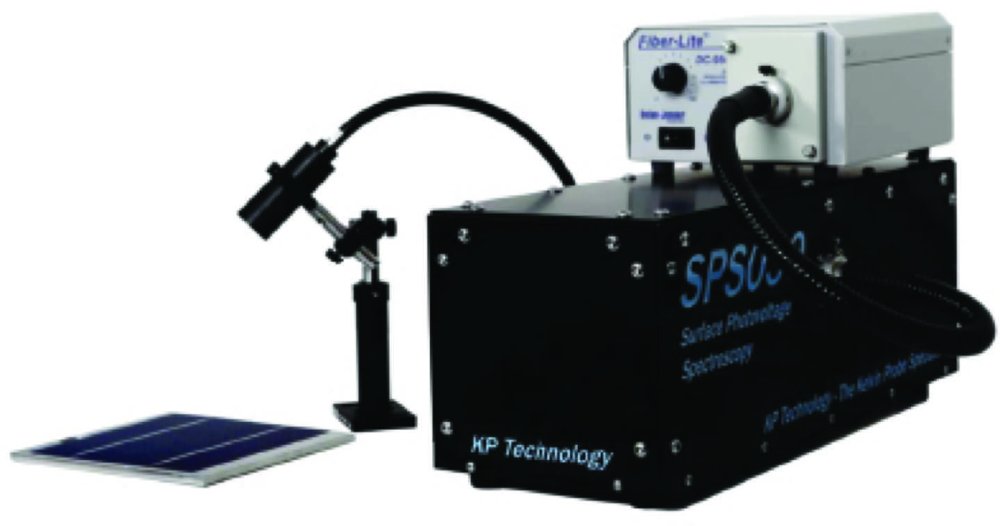
The surface photovoltage spectroscopy modules are the perfect all-in-one solution for in-depth studies of light sensitive materials such as organic semiconductors, solar cells or light sensitive dyes. The modules offer a comprehensive range of measurement modes including DC and AC surface photovoltage studies utilising the built-in optical chopper. Total digital control of all parameters including light intensity and wavelength (400 - 700 nm: SPS030 or 400 - 1000 nm: SPS040) gives the opportunity to investigate and characterise the surface photovoltage and surface photovoltage spectroscopy properties of samples. The latest materials and applications highlighted in published papers includes, gold films, perovskite solar cells, titanium dioxide nanotubes, dye sensitised solar cells, hybrid organic/inorganic photocathodes and tungsten trioxide. Download the product brochure for more information on the Surface Photovoltage range, including technical specifications, example measurements and add-on options. - SPS030 - SPS040 - SPV020
CATEGORY
The surface photovoltage spectroscopy modules are the perfect all-in-one solution for in-depth studies of light sensitive materials such as organic semiconductors, solar cells or light sensitive dyes. The modules offer a comprehensive range of measurement modes including DC and AC surface photovoltage studies utilising the built-in optical chopper. Total digital control of all parameters including light intensity and wavelength (400 - 700 nm: SPS030 or 400 - 1000 nm: SPS040) gives the opportunity to investigate and characterise the surface photovoltage and surface photovoltage spectroscopy properties of samples. The latest materials and applications highlighted in published papers includes, gold films, perovskite solar cells, titanium dioxide nanotubes, dye sensitised solar cells, hybrid organic/inorganic photocathodes and tungsten trioxide. Download the product brochure for more information on the Surface Photovoltage range, including technical specifications, example measurements and add-on options.
CATEGORY
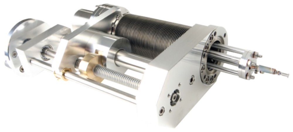
Specification - Tip material / diameter: 4 mm - 10 mm stainless steel tip (other diameters available) - Work function resolution: 1 - 3 meV - Standard translator: 50 mm manual translator - Motorised translator sizes: 50 mm or 100 mm manual translators - Height control (auto): Approximately 1 - 5 mm by DC offset (unless motorized) - Visualisation: Single-point work function/contact potential difference scans - Oscilloscope: Digital TFT oscilloscope for real time signal - Options: SPS/SPV/APS capabilities - Test sample: Available on request - Control supplied: USB control with dedicated software - Detection system: Off-null with parasitic capacity rejection - Mounting geometry: Normal to sample surface - Mounting port: DN40/CF70 (2.75 inch) OD - Vacuum compatibility: 2 x 10-11 mBar - Flange to sample distance: User defined - UHV cell: Not included - Warranty: 12 Months
CATEGORY
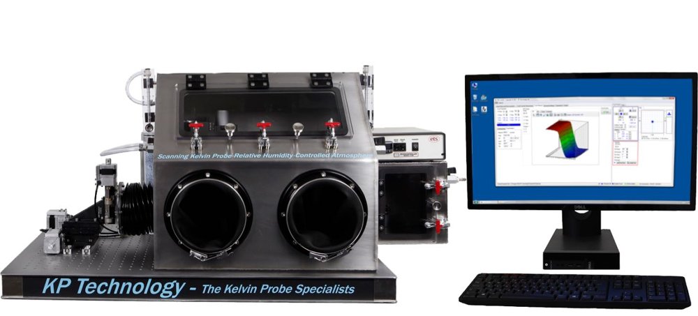
Specification Tip material / diameter: 2 mm stainless steel tip Work function resolution: 1 - 3 meV Sample scanning: 50 x 50 mm Relative humidity control: Automatic: 20 - 80% Atmospheric control: Oxygen <1% Optical system: Colour Camera Oscilloscope: Digital TFT oscilloscope for real time signal Test sample: Gold and aluminium sample Breadboard footprint: 900 x 600 mm Control supplied: PC with dedicated software Detection system: Off-null with parasitic capacity rejection Warranty: 12 Months
CATEGORY
