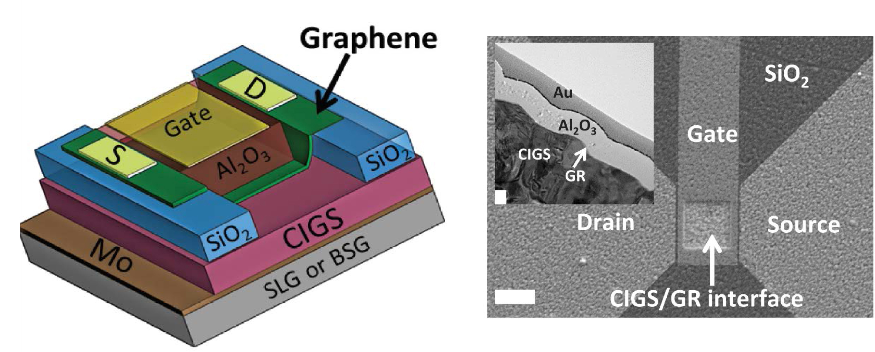
Graphene, the two-dimensional powerhouse, packs extreme durability, electrical conductivity, and transparency into a one-atom-thick sheet of carbon. Despite being heralded as a breakthrough "wonder material," graphene has been slow to leap into commercial and industrial products and processes.
Now, scientists have developed a simple and powerful method for creating resilient, customized, and high-performing graphene: layering it on top of common glass. This scalable and inexpensive process helps pave the way for a new class of microelectronic and optoelectronic devices—everything from efficient solar cells to touch screens.
"We believe that this work could significantly advance the development of truly scalable graphene technologies."— Brookhaven Lab and Stony Brook University physicist Matthew Eisaman
The collaboration—led by scientists at the U.S. Department of Energy's (DOE) Brookhaven National Laboratory, Stony Brook University (SBU), and the Colleges of Nanoscale Science and Engineering at SUNY Polytechnic Institute—published their results February 12, 2016, in the journal Scientific Reports.
"We believe that this work could significantly advance the development of truly scalable graphene technologies," said study coauthor Matthew Eisaman, a physicist at Brookhaven Lab and professor at SBU.
The scientists built the proof-of-concept graphene devices on substrates made of soda-lime glass—the most common glass found in windows, bottles, and many other products. In an unexpected twist, the sodium atoms in the glass had a powerful effect on the electronic properties of the graphene.
"The sodium inside the soda-lime glass creates high electron density in the graphene, which is essential to many processes and has been challenging to achieve," said coauthor Nanditha Dissanayake of Voxtel, Inc., but formerly of Brookhaven Lab. "We actually discovered this efficient and robust solution during the pursuit of something a bit more complex. Such surprises are part of the beauty of science."
Crucially, the effect remained strong even when the devices were exposed to air for several weeks—a clear improvement over competing techniques.
The experimental work was done primarily at Brookhaven's Sustainable Energy Technologies Department and the Center for Functional Nanomaterials (CFN), which is a DOE Office of Science User Facility.
The graphene tweaks in question revolve around a process called doping, where the electronic properties are optimized for use in devices. This adjustment involves increasing either the number of electrons or the electron-free "holes" in a material to strike the perfect balance for different applications. For successful real-world devices, it is also very important that the local number of electrons transferred to the graphene does not degrade over time.
"The graphene doping process typically involves the introduction of external chemicals, which not only increases complexity, but it can also make the material more vulnerable to degradation," Eisaman said. "Fortunately, we found a shortcut that overcame those obstacles."
The team initially set out to optimize a solar cell containing graphene stacked on a high-performance copper indium gallium diselenide (CIGS) semiconductor, which in turn was stacked on an industrial soda-lime glass substrate.
The scientists then conducted preliminary tests of the novel system to provide a baseline for testing the effects of subsequent doping. But these tests exposed something strange: the graphene was already optimally doped without the introduction of any additional chemicals.
"To our surprise, the graphene and CIGS layers already formed a good solar cell junction!" Dissanayake said. "After much investigation, and the later isolation of graphene on the glass, we discovered that the sodium in the substrate automatically created high electron density within our multi-layered graphene."
Pinpointing the mechanism by which sodium acts as a dopant involved a painstaking exploration of the system and its performance under different conditions, including making devices and measuring the doping strength on a wide range of substrates, both with and without sodium.
"Developing and characterizing the devices required complex nanofabrication, delicate transfer of the atomically thin graphene onto rough substrates, detailed structural and electro-optical characterization, and also the ability to grow the CIGS semiconductor," Dissanayake said.
"Fortunately, we had both the expertise and state-of-the-art instrumentation on hand to meet all those challenges, as well as generous funding."
The bulk of the experimental work was conducted at Brookhaven Lab using techniques developed in-house, including advanced lithography. For the high-resolution electron microscopy measurements, CFN staff scientists and study coauthors Kim Kisslinger and Lihua Zhang lent their expertise. Coauthors Harry Efstathiadis and Daniel Dwyer—both at the College of Nanoscale Science and Engineering at SUNY Polytechnic Institute—led the effort to grow and characterize the high-quality CIGS films.
"Now that we have demonstrated the basic concept, we want to focus next on demonstrating fine control over the doping strength and spatial patterning," Eisaman said.
The scientists now need to probe more deeply into the fundamentals of the doping mechanism and more carefully study material's resilience during exposure to real-world operating conditions. The initial results, however, suggest that the glass-graphene method is much more resistant to degradation than many other doping techniques.
"The potential applications for graphene touch many parts of everyone's daily life, from consumer electronics to energy technologies," Eisaman said. "It's too early to tell exactly what impact our results will have, but this is an important step toward possibly making some of these applications truly affordable and scalable."
For example, graphene's high conductivity and transparency make it a very promising candidate as a transparent, conductive electrode to replace the relatively brittle and expensive indium tin oxide (ITO) in applications such as solar cells, organic light emitting diodes (OLEDs), flat panel displays, and touch screens. In order to replace ITO, scalable and low-cost methods must be developed to control graphene's resistance to the flow of electrical current by controlling the doping strength. This new glass-graphene system could rise to that challenge, the researchers say.
The work at Brookhaven Lab was funded through Brookhaven Lab's Sustainable Energy Technologies Department by the DOE Office of Science and by Brookhaven's Laboratory Directed Research and Development (LDRD) Program. The CFN at Brookhaven is supported by the DOE Office of Science (BES).
Brookhaven National Laboratory
#Graphene #Nanoelectronics

Waste polyamide-derived CQDs show continuous photoluminescence tuning from 308 to 552 nm through sequential defect-state engineering, with optical transition energies decreasing from 4.32 to 2.50 eV. @Christian Ebere Enyoh from Saitama University Carbon quantum dots (CQDs) are fluorescent carbon nanomaterials with potential applications in sensing, optoelectronics, displays, anti-counterfeiting, and environmental technologies. Their optical properties can be adjusted by modifying the carbon...

The researchers used circularly polarized light at normal incidence and found that helicity-dependent photocurrents appeared perpendicular to the crystal’s polarization but vanished when measured parallel to it, supporting a bulk origin of CPGE. @Institute of Science Tokyo The circular photogalvanic effect (CPGE), a phenomenon that generates helicity-dependent photocurrents in noncentrosymmetric materials, can originate purely from a crystal's internal structure without contribution from the...

Summary of gold nanoparticle growth programming in liposome based on localization of biomineralization peptide The position of biomineralization peptides within liposomes can influence how gold nanoparticles grow, reports a research team from Institute of Science Tokyo. Peptides localized at the membrane interface promote branched structures, while those confined to the liposome interior favor spherical nanoparticles. The findings offer a new strategy for controlling nanoscale reaction...
