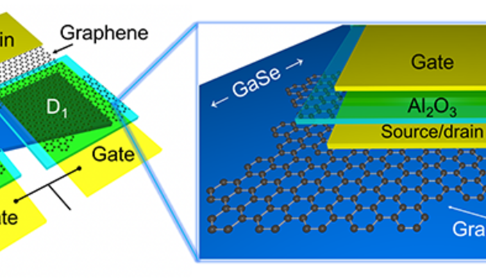
The 2D material device designed and fabricated by Aalto University's researchers may prove useful in wearable electronics and sensors.
Graphene has been predicted to revolutionise electronics since Andre Geim and Konstantin Novoselovreceived the Nobel Prize in physics in 2010 for the breakthrough experiments conducted with the material.
Graphene is a so-called 2D material, that is, it is only one atom thick film. Graphite, which is a well-known material, consists of huge number of graphene layers on top of each other. Despite being ultimately thin, graphene is an excellent conductor of electricity and heat, and it is extremely durable. However, its band gap is zero, which limits its application in some semiconductor applications as it results in low intrinsic on/off ratio. Now Aalto University's researchers have managed to fabricate an electricity-conducting material combination with especially promising properties by merging graphene and another 2D material, gallium selenide. In the semiconductor industry this kind of structure is known as a heterojunction. The results were recently published in the Advanced Materials science journal.
'This is the first time when gallium selenide is used with graphene. This kind of new heterojunctions will be important in future as conventional heterojunctions are already vital part of current semiconductor industry forming the basis for example for lasers and transistors.', explains Juha Riikonen, head of the research group.
'Because the component is made of 2D materials, it is, in comparison with those containing silicon, extremely thin, approximately one ten-thousandth part of the diameter of a single hair', post-doctoral researcher Wonjae Kim explains.
In earlier research, the 2D structures combined with graphene were fabricated manually, layer by layer, which made the process slow, challenging and difficult to scale. The component structure developed by Riikonen, Kim and their colleagues utilized elements from both lateral and vertical device design enabling the use of standard fabrication methods utilized in the semiconductor industry instead of laborious manual fabrication.
'Our inspiration comes from the existing silicon technology and we want to bring out the state-of-the-art fabrication of 2D material devices from research labs to industry. In addition to new and simpler way of manufacturing, our components have excellent characteristics. For example, the on/off ratio, which is critical parameter in electronics, is over 10³. This underscores the feasibility of both GaSe and the device concept', Kim sums up.
'Being transparent and thin, 2D components open completely new possibilities for the development of electronics. They would be suitable for example for wearable electronics, and they could be placed on spectacles and windows. Moreover, the components are suitable for various sensors', he envisages.
Abstract of the article http://onlinelibrary.wiley.com/doi/10.1002/adma.201504514/abstract
Aalto
#Graphene #2DMaterials #Sensors #MaterialScience
SPECS reports on work at the LMA microscopy lab, where Dr. David Serrate's team used the JT-STM to study graphene nanoribbons on MgO/Ag(001) and the Aarhus 150 to monitor nanostructure growth.
Nanologica's board has resolved on a rights issue of units of appx. SEK 110.5 million, with an oversubscription option of up to SEK 10 million. Commitments and a guarantee intention cover appx. SEK 85.7 million.
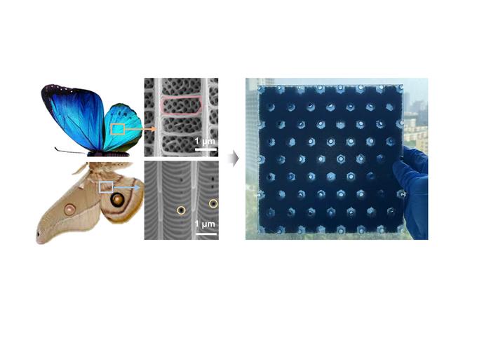
Researchers at Harbin Institute of Technology have printed a 24 mm metamaterial that absorbs impact, shields microwaves and damps low-frequency noise at once. Inspired by butterfly wing scales, it nests a gyroid lattice inside a hexagonal honeycomb, absorbing 21.9 times more impact energy than an equal-weight honeycomb and capturing over 90% of 2-40 GHz radiation and 600-900 Hz sound.
This week in nanotech
$108.5M raised
8 funding rounds · 44 deals tracked
New products
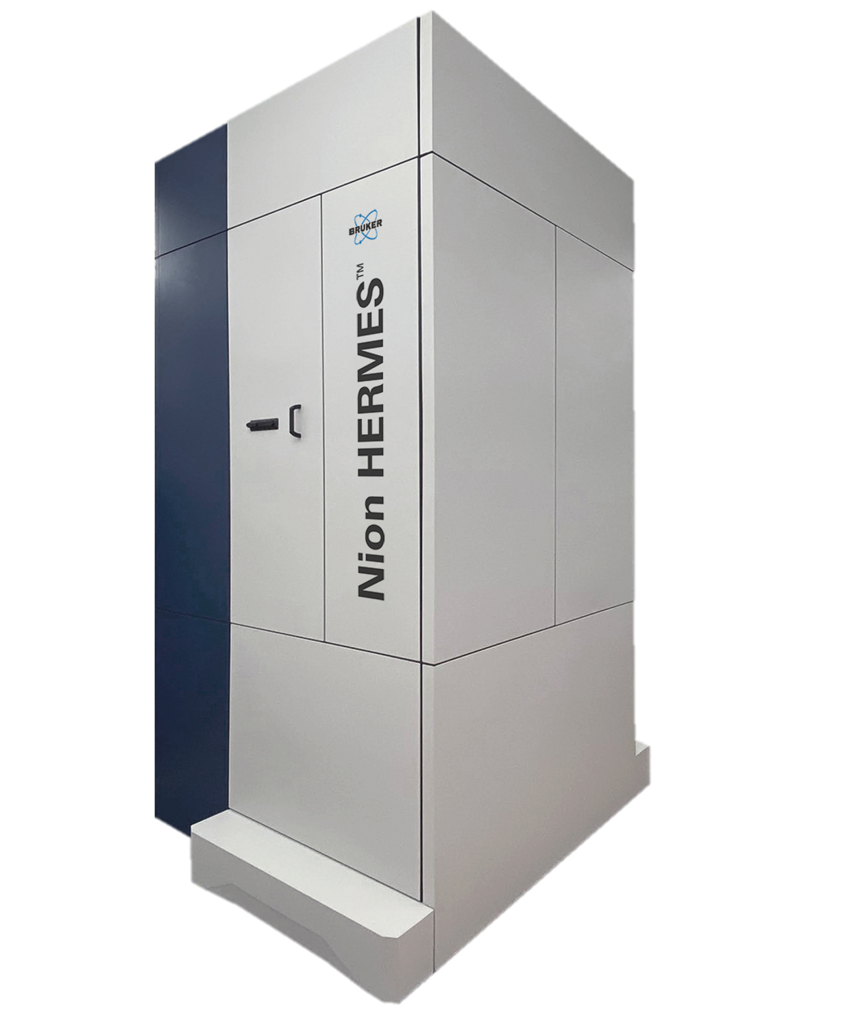 Nion-compatible In Situ STEM Holders for Electrical BiasingHummingbird Scientific Featured
 Ti-WCMBN Nanomaterialia Featured
 Talphene™ Graphene AdditivesTalga Group
Market insights
Last 30 days: Quantum Technologies drew the most money: $3.17B.
Money raised per month
Behind the deal
Who invested in Photon Bridge’s $11.2M Series A?
See the investors with Insights Pro →