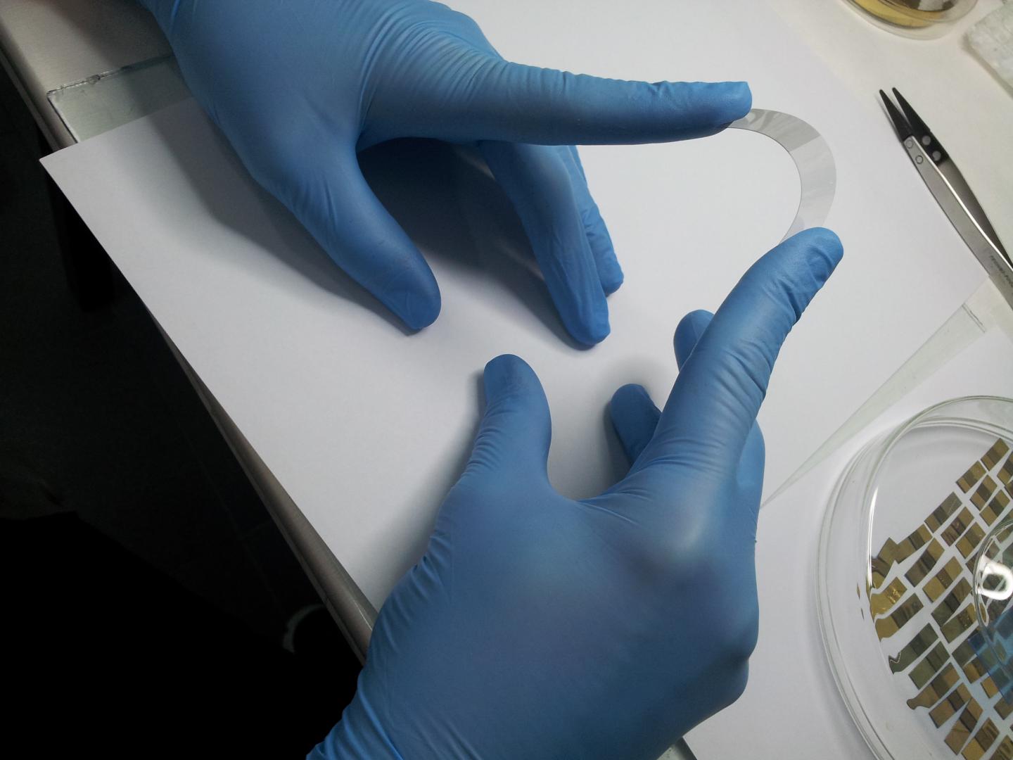
Superconductors' never-ending flow of electrical current could provide new options for energy storage and superefficient electrical transmission and generation, to name just a few benefits. But the signature zero electrical resistance of superconductors is reached only below a certain critical temperature, hundreds of degrees Celsius below freezing, and is very expensive to achieve.
Physicists from the University of Belgrade in Serbia believe they've found a way to manipulate superthin, waferlike monolayers of superconductors, such as graphene, a monolayer of carbon, thus changing the material's properties to create new artificial materials for future devices. The findings from the group's theoretical calculations and experimental approaches are published in the Journal of Applied Physics, from AIP Publishing.
"The application of tensile biaxial strain leads to an increase of the critical temperature, implying that achieving high temperature superconductivity becomes easier under strain," said the study's first author from the University of Belgrade's LEX Laboratory, Vladan Celebonovic.
The team examined how conductivity within low-dimensional materials, such as lithium-doped graphene, changed when different types of forces applied a "strain" on the material. Strain engineering has been used to fine-tune the properties of bulkier materials, but the advantage of applying strain to low-dimensional materials, only one atom thick, is that they can sustain large strains without breaking.
Conductivity depends on the movement of electrons, and although it took seven months of hard work to accurately derive the math to describe this movement in the Hubbard model, the team was finally able to theoretically examine electron vibration and transport. These models, alongside computational methods, revealed how strain introduces critical changes to doped-graphene and magnesium-diboride monolayers.
"Putting a low-dimensional material under strain changes the values of all the material parameters; this means there's the possibility of designing materials according to our needs for all kind of applications," said Celebonovic, who explained that combining the manipulation of strain with the chemical adaptability of graphene gives the potential for a large range of potential new materials. Given the high elasticity, strength and optical transparency of graphene, the applicability could be far reaching -- think flexible electronics and optoelectric devices.
Going a step further, Celebonovic and colleagues tested how two different approaches to strain engineering thin monolayers of graphene affected the 2D material's lattice structure and conductivity. For liquid-phase "exfoliated" graphene sheets, the team found that stretching strains pulled apart individual flakes and so increased the resistance, a property that could be used to make sensors, such as touch screens and e-skin, a thin electronic material that mimics the functionalities of human skin.
"In the atomic force microscopy study on micromechanically exfoliated graphene samples, we showed that the produced trenches in graphene could be an excellent platform in order to study local changes in graphene conductivity due to strain. And those results could be related to our theoretical prediction on effects of strain on conductivity in one-dimensional-like systems," said Jelena Pesic, another author on the paper, from the University of Belgrade's Graphene Laboratory.
Although the team foresees many challenges to realizing the theoretical calculations from this paper experimentally, they are excited that their work could soon "revolutionize the field of nanotechnology."
Selected transport, vibrational, and mechanical properties of low-dimensional systems under strain
V. Celebonovic, J. Pesic, R. Gajic, B. Vasic, and A. Matkovic
Journal of Applied Physics 125, 154301 (2019)
DOI: https://doi.org/10.1063/1.5054120
University of Belgrade
#2DMaterials #Nanomanufacturing #Nanoengineering #Graphene

Waste polyamide-derived CQDs show continuous photoluminescence tuning from 308 to 552 nm through sequential defect-state engineering, with optical transition energies decreasing from 4.32 to 2.50 eV. @Christian Ebere Enyoh from Saitama University Carbon quantum dots (CQDs) are fluorescent carbon nanomaterials with potential applications in sensing, optoelectronics, displays, anti-counterfeiting, and environmental technologies. Their optical properties can be adjusted by modifying the carbon...

The researchers used circularly polarized light at normal incidence and found that helicity-dependent photocurrents appeared perpendicular to the crystal’s polarization but vanished when measured parallel to it, supporting a bulk origin of CPGE. @Institute of Science Tokyo The circular photogalvanic effect (CPGE), a phenomenon that generates helicity-dependent photocurrents in noncentrosymmetric materials, can originate purely from a crystal's internal structure without contribution from the...

Summary of gold nanoparticle growth programming in liposome based on localization of biomineralization peptide The position of biomineralization peptides within liposomes can influence how gold nanoparticles grow, reports a research team from Institute of Science Tokyo. Peptides localized at the membrane interface promote branched structures, while those confined to the liposome interior favor spherical nanoparticles. The findings offer a new strategy for controlling nanoscale reaction...
