DOE's Lawrence Berkeley National Laboratory
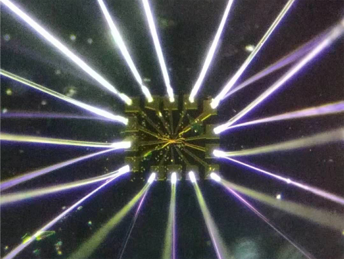
Ever since graphene's discovery in 2004, scientists have looked for ways to put this talented, atomically thin 2D material to work. Thinner than a single strand of DNA yet 200 times stronger than steel, graphene is an excellent conductor of electricity and heat, and it can conform to any number of shapes, from an ultrathin 2D sheet, to an electronic circuit.
Last year, a team of researchers led by Feng Wang, a faculty scientist in Berkeley Lab's Materials Sciences Division and a professor of physics at UC Berkeley, developed a multitasking graphene device that switches from a superconductor that efficiently conducts electricity, to an insulator that resists the flow of electric current, and back again to a superconductor.
Now, as reported in the journal Nature, the researchers have tapped into their graphene system's talent for juggling not just two properties, but three: superconducting, insulating, and a type of magnetism called ferromagnetism. The multitasking device could make possible new physics experiments, such as research in the pursuit of an electric circuit for faster, next-generation electronics like quantum computing technologies.
"So far, materials simultaneously showing superconducting, insulating, and magnetic properties have been very rare. And most people believed that it would be difficult to induce magnetism in graphene, because it's typically not magnetic. Our graphene system is the first to combine all three properties in a single sample," said Guorui Chen, a postdoctoral researcher in Wang's Ultrafast Nano-Optics Group at UC Berkeley, and the study's lead author.
Using electricity to turn on graphene's hidden potential
Graphene has a lot of potential in the world of electronics. Its atomically thin structure, combined with its robust electronic and thermal conductivity, "could offer a unique advantage in the development of next-generation electronics and memory storage devices," said Chen, who also worked as a postdoctoral researcher in Berkeley Lab's Materials Sciences Division at the time of the study.
The problem is that the magnetic materials used in electronics today are made of ferromagnetic metals, such as iron or cobalt alloys. Ferromagnetic materials, like the common bar magnet, have a north and a south pole. When ferromagnetic materials are used to store data on a computer's hard disk, these poles point either up or down, representing zeros and ones - called bits.
Graphene, however, is not made of a magnetic metal - it's made of carbon.
So the scientists came up with a creative workaround.
They engineered an ultrathin device, just 1 nanometer in thickness, featuring three layers of atomically thin graphene. When sandwiched between 2D layers of boron nitride, the graphene layers - described as trilayer graphene in the study - form a repeating pattern called a moiré superlattice.
By applying electrical voltages through the graphene device's gates, the force from the electricity prodded electrons in the device to circle in the same direction, like tiny cars racing around a track. This generated a forceful momentum that transformed the graphene device into a ferromagnetic system.
More measurements revealed an astonishing new set of properties: The graphene system's interior had not only become magnetic but also insulating; and despite the magnetism, its outer edges morphed into channels of electronic current that move without resistance. Such properties characterize a rare class of insulators known as Chern insulators, the researchers said.
Even more surprising, calculations by co-author Ya-Hui Zhang of the Massachusetts Institute of Technology revealed that the graphene device has not just one, but two conductive edges, making it the first observed "high-order Chern insulator," a consequence of the strong electron-electron interactions in the trilayer graphene.
Scientists have been in hot pursuit of Chern insulators in a field of research known as topology, which investigates exotic states of matter. Chern insulators offer potential new ways to manipulate information in a quantum computer, where data is stored in quantum bits, or qubits. A qubit can represent a one, a zero, or a state in which it is both a one and a zero at the same time.
"Our discovery demonstrates that graphene is an ideal platform for studying different physics, ranging from single-particle physics, to superconductivity, and now topological physics to study quantum phases of matter in 2D materials," Chen said. "It's exciting that we can now explore new physics in a tiny device just 1 millionth of a millimeter thick."
The researchers hope to conduct more experiments with their graphene device to have a better understanding of how the Chern insulator/magnet emerged, and the mechanics behind its unusual properties.
Tunable correlated Chern insulator and ferromagnetism in a moiré superlattice
Guorui Chen, Aaron L. Sharpe, Eli J. Fox, Ya-Hui Zhang, Shaoxin Wang, Lili Jiang, Bosai Lyu, Hongyuan Li, Kenji Watanabe, Takashi Taniguchi, Zhiwen Shi, T. Senthil, David Goldhaber-Gordon, Yuanbo Zhang, Feng Wang
Nature, 2020; 579 (7797): 56
DOI: 10.1038/s41586-020-2049-7
Contact information:
Feng Wang
UC Berkeley professor of physics & faculty scientist in LBL's Materials Sciences Division
fengwang76@berkeley.edu
Phone: (510) 643-3275

Waste polyamide-derived CQDs show continuous photoluminescence tuning from 308 to 552 nm through sequential defect-state engineering, with optical transition energies decreasing from 4.32 to 2.50 eV. @Christian Ebere Enyoh from Saitama University Carbon quantum dots (CQDs) are fluorescent carbon nanomaterials with potential applications in sensing, optoelectronics, displays, anti-counterfeiting, and environmental technologies. Their optical properties can be adjusted by modifying the carbon...

The researchers used circularly polarized light at normal incidence and found that helicity-dependent photocurrents appeared perpendicular to the crystal’s polarization but vanished when measured parallel to it, supporting a bulk origin of CPGE. @Institute of Science Tokyo The circular photogalvanic effect (CPGE), a phenomenon that generates helicity-dependent photocurrents in noncentrosymmetric materials, can originate purely from a crystal's internal structure without contribution from the...

Summary of gold nanoparticle growth programming in liposome based on localization of biomineralization peptide The position of biomineralization peptides within liposomes can influence how gold nanoparticles grow, reports a research team from Institute of Science Tokyo. Peptides localized at the membrane interface promote branched structures, while those confined to the liposome interior favor spherical nanoparticles. The findings offer a new strategy for controlling nanoscale reaction...
