Delft-based Delmic has launched AURORA, a system that automatically detects crystal defects in new chip materials. The company says the tool makes hidden defects in materials such as silicon carbide and gallium nitride visible during wafer inspection.
AURORA uses cathodoluminescence. An electron microscope scans the material with a fine electron beam, causing it to emit light. Where the crystal is flawed, the light becomes weaker or shifts in colour. A sensitive mirror collects the light and produces a map of the wafer showing defects, strain and dopant variations at the nanoscale.
The system aligns the mirror itself and stays in focus even when the wafer is slightly warped. It then runs a predefined measurement recipe unattended across large areas of wafers up to 300 millimetres in diameter, depending on the microscope. Accompanying software counts and analyses the defects found, so manufacturers can trace whether a defect originated in the substrate or later in the process.
AURORA is retrofitted to an electron microscope rather than sold as a standalone tool. "AURORA works with most commercial large-chamber microscopes," said Sander den Hoedt, co-founder and CEO of Delmic. "When the mirror is retracted, the microscope remains available for other work."
Den Hoedt said silicon is reaching its limits for converting large amounts of power, and that silicon carbide and gallium nitride chips lose less energy and handle higher voltages and temperatures. The crystals of these materials are difficult to grow without flaws, and standard inspection often misses defects. "The companies that learn fastest what happens inside those crystals will set the pace for electric mobility, clean energy and AI," he said.
AURORA will be available from Q1 2027 in four standard configurations, each optimised for a different class of materials, from ultraviolet-emitting semiconductors to infrared applications. Mirrors, filters and detectors can be upgraded or exchanged later. Delmic engineers install the system on the customer's microscope and train users on site.
Source: Delmic news
AIXTRON SE reported Q3 2026 order intake of EUR 274.9 million, up 122% year-on-year, with optoelectronics at about 68% of equipment orders. Revenue reached EUR 183.6 million and full-year guidance was confirmed.
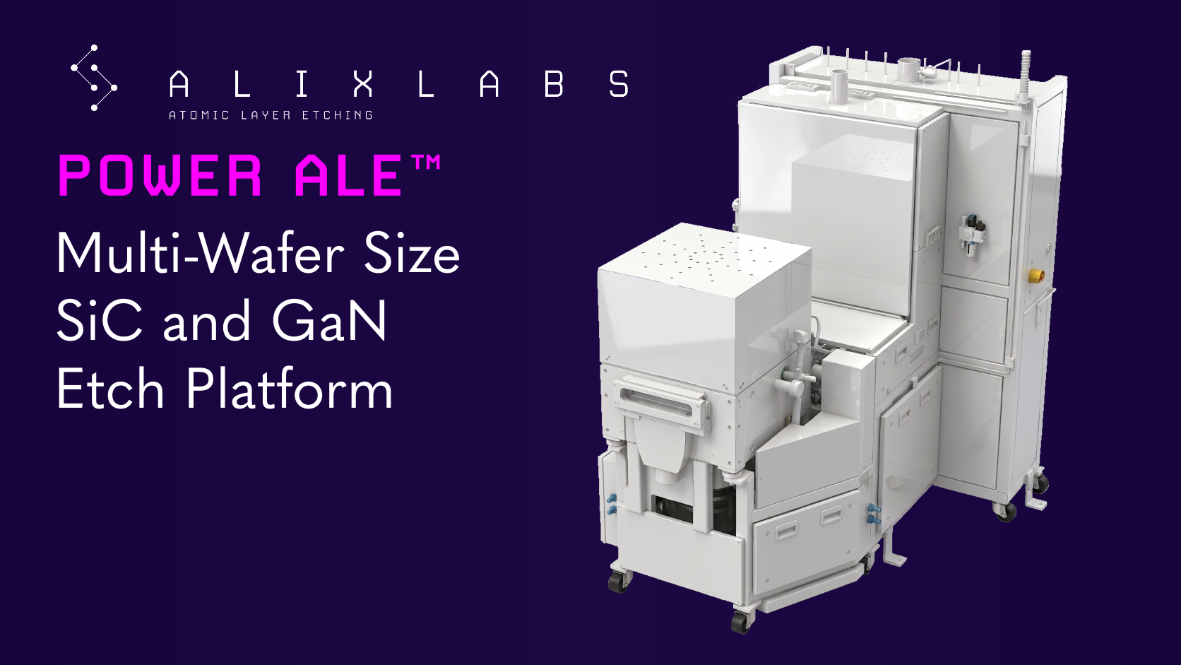
AlixLabs has introduced Power ALE™, an Atomic Layer Etching platform for wide-bandgap power semiconductors. It supports 150, 200 and 300 mm wafers and targets SiC trench sidewall smoothing and GaN HEMT gate recess.
MRDI will lead and operate Hong Kong's first national manufacturing innovation centre, supported by the region's First Five-Year Plan and 2026 Policy Address. The institute is installing two pilot lines for third-generation semiconductor chips at the Yuen Long InnoPark.
This week in nanotech
$118.9M raised
5 funding rounds · 36 deals tracked
New products
 Ti-WCMBN Nanomaterialia Featured
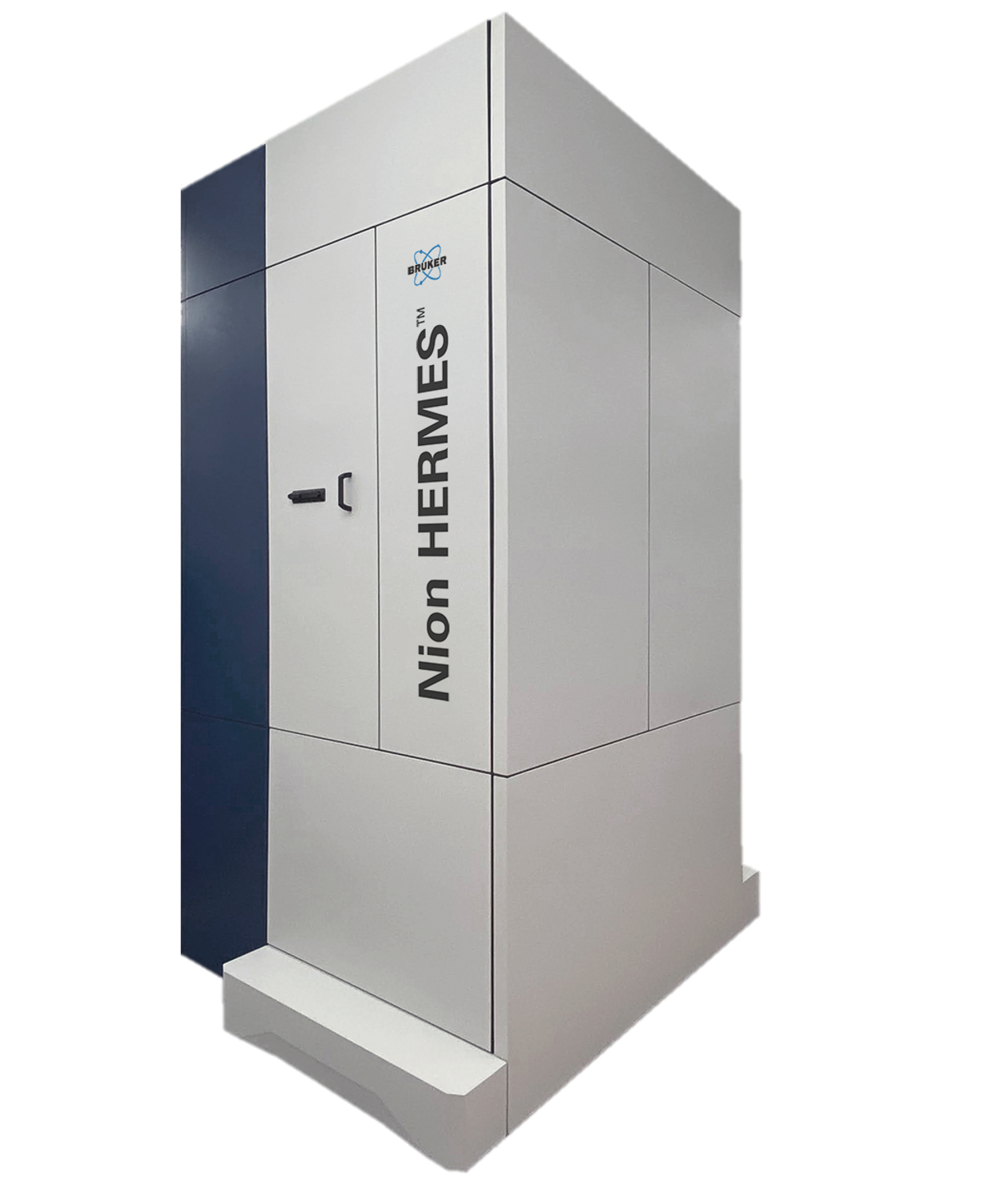 Nion-compatible In Situ STEM Holders for Electrical BiasingHummingbird Scientific Featured
 GiiiGii
Market insights
Last 30 days: Semiconductors & Electronics was the busiest vertical: 51 of 165 events (31%).
Money raised per month