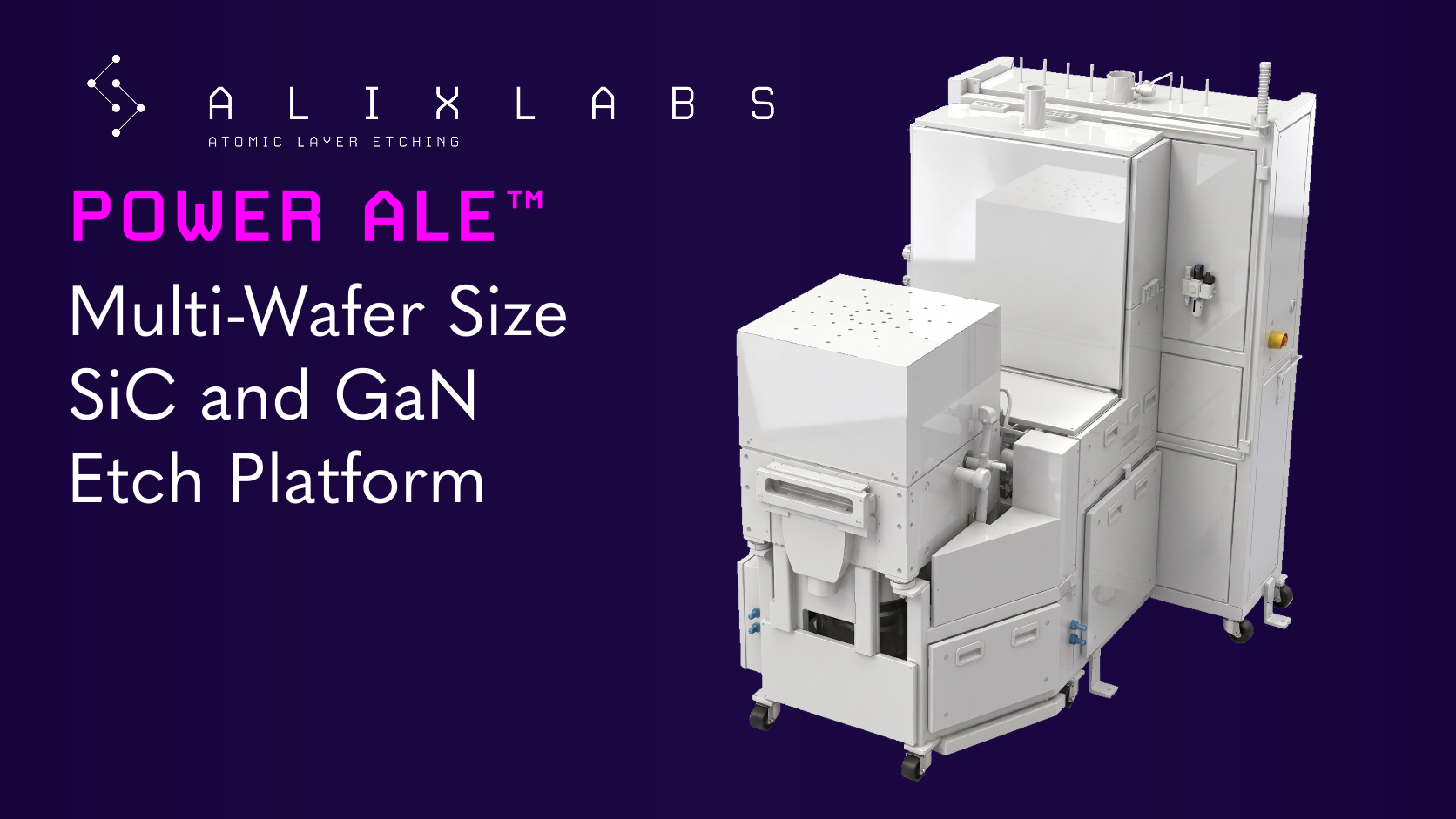
26 October 2026. AlixLabs AB has introduced Power ALE™, its application of Atomic Layer Etching to wide-bandgap power semiconductor manufacturing, with an initial focus on SiC and direct applicability to GaN. The platform combines Atomic Layer Etching with a semiconductor-fab-compatible hardware and software architecture. The equipment is built around a 300 mm platform while supporting 150, 200 and 300 mm wafers, corresponding to 6-, 8- and 12-inch formats.
The system uses a vertically configured plasma chamber that combines an inductively coupled plasma (ICP) source with independently controlled wafer bias. Both RF sources support pulsed operation and synchronization. The chamber integrates independent active thermal management across the pedestal, showerhead, walls and lid. Substrates are held by mechanical clamping or an optional electrostatic chuck (ESC), and yttria-coated field-replaceable liners provide plasma confinement. A modular gas system isolates corrosive gas delivery from non-corrosive gases and enables sub-10 ms dosing.
For SiC, Power ALE™ can support plasma etching, trench profile engineering, sidewall smoothing and surface conditioning. In AlixLabs SiC work, the as-received trench sidewall had an Sa of approximately 0.95 nm and Sq of 1.22 nm. Two optimized ALE processes reduced Sa to approximately 0.49-0.50 nm and Sq to approximately 0.61-0.64 nm, roughly a 47-48 percent reduction in average sidewall roughness. Cross-sectional SEM analysis indicates minimal impact on the overall trench profile.
For GaN, the architecture can support precision GaN and AlGaN etching, E-mode HEMT gate recess, surface smoothing and preparation of sensitive semiconductor interfaces. AlixLabs reports GaN surface Rq decreasing from approximately 0.13 nm to 0.070 nm after Power ALE™, and SiC Rq decreasing from approximately 0.162 nm to 0.071 nm in the examples presented. The company states that the eventual improvement in finished SiC device characteristics still needs to be established through device fabrication and electrical characterization.
AlixLabs is also developing ALE for GaN surface smoothing, SiNx processing and more advanced GaN structures. Its work within the EU funded ALL2GaN program includes GaN-on-SiC, D-mode and E-mode HEMTs, alternative substrates and emerging vertical and nanostructured GaN device concepts. The equipment uses a production-grade load-lock and robotic wafer-handling platform, and the 300 mm automation architecture can be adapted to smaller wafer formats.
Source: AlixLabs AB news
MRDI will lead and operate Hong Kong's first national manufacturing innovation centre, supported by the region's First Five-Year Plan and 2026 Policy Address. The institute is installing two pilot lines for third-generation semiconductor chips at the Yuen Long InnoPark.
Wolfspeed announced a conditional loan commitment letter from the U.S. Department of War for up to $1.5 billion of long-term financing for silicon carbide materials and wide bandgap power devices.
Infineon will supply its first 900 V GaN monolithic bidirectional switches to Enphase Energy for solid-state transformer power modules. The devices have been tested and are being integrated into Enphase's IQ SST product development.
This week in nanotech
$281.1M raised
6 funding rounds · 36 deals tracked
New products
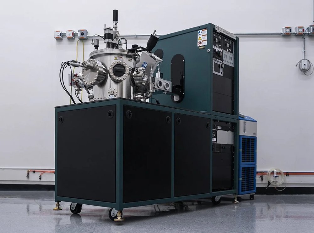 Orion Sputtering Deposition SystemsAJA International Featured
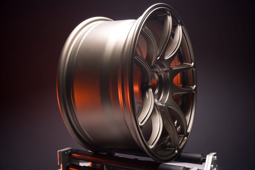 Ti-WCMBN Nanomaterialia Featured
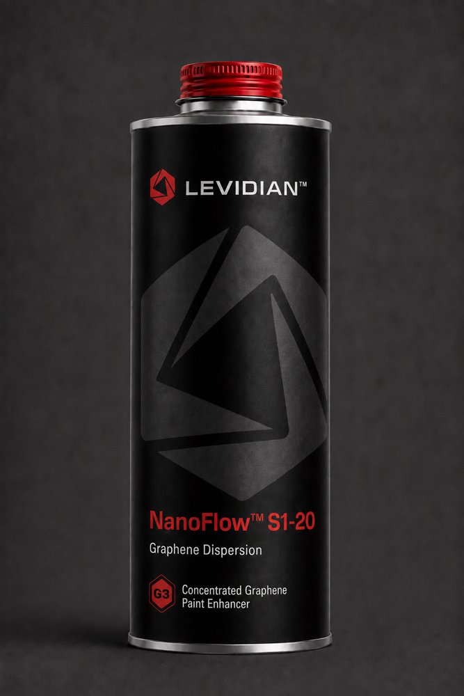 NanoFlow® S1-20Levidian
Market insights
Last 30 days: Quantum Technologies drew the most money: $3.17B.
Money raised per month
Behind the deal
Who led Institut de Microelectronica de Barcelona (IMB-CNM, CSIC)’s $185.7M Grant?
See the investors with Insights Pro →