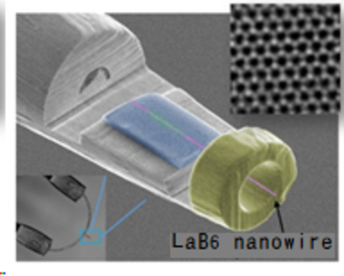
The National Institute for Materials Science (NIMS) and JEOL, Ltd. have developed a lanthanum hexaboride (LaB6) nanowire-based field emission gun that is installable on an aberration-corrected transmission electron microscope (TEM). This combined unit is able to perform atomic resolution observation at an energy resolution of 0.2 eV—the highest resolution ever recorded for non-monochromatic electron guns—with a high current stability of 0.4%.
Unsuccessful efforts have been made for more than 20 years to develop field emission guns using theoretically high-performance nano materials. It has been found challenging to integrate a nanowire-based field emission gun into an electron microscope without undermining its physical properties, such as lives and stability. For this reason, commercially available field emission guns are still equipped with tungsten needles developed more than half a century ago.
This NIMS-JEOL research team 1) developed techniques to chemically synthesize and grow high-purity, single-crystal nanowires of LaB6, known to be an excellent electron-emitting hot cathode material, 2) designed an electron source mechanism capable of efficiently emitting electrons and 3) developed techniques to extract a single nanowire and integrate it into an optimized electron source structure.
The LaB6 nanowire-based electron source has a number of advantages: relatively moderate vacuum condition requirements, very high current stability, low extraction voltage, narrow electron beam energy distribution width and high brightness. This electron source may be applicable to the development of next-generation field emission electron microscopes with higher spatial and energy resolution—potentially valuable tools in the semiconductor and medical fields.
This project was carried out by a team of NIMS researchers (Han Zhang, Cretu Ovidiu, Koji Kimoto, Takeshi Kasaya, Hideki T. Miyazaki, Naohito Tsujii, Hongxin Wang, Yasushi Yamauchi and Daisuke Fujita) and JEOL researchers (Yu Jimbo, Akira Niwata, Akihiro Ikeda, Akira Yasuhara, Shin-ichi Kitamura and Hironobu Manabe).
National Institute for Materials Science (Japan)
Reference
High-endurance micro-engineered LaB6 nanowire electron source for high-resolution electron microscopy
Han Zhang, Yu Jimbo, Akira Niwata, Akihiro Ikeda, Akira Yasuhara, Cretu Ovidiu, Koji Kimoto, Takeshi Kasaya, Hideki T. Miyazaki, Naohito Tsujii, Hongxin Wang, Yasushi Yamauchi, Daisuke Fujita, Shin-ichi Kitamura & Hironobu Manabe
Nature Nanotechnology (2021) DOI: 10.1038/s41565-021-00999-w
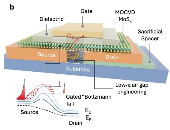
Researchers have fabricated transistors from molybdenum disulfide, an atomically thin two dimensional semiconductor, with channel lengths below five nanometers. An air gap beneath the channel lets the gate keep tighter control of current and curb leakage, delivering switching performance beyond silicon's theoretical limit at comparable size. The devices were built across a four inch wafer, pointing to manufacturability.
nanoComposix has expanded its Quality Management System to include ISO 13485:2016 certification. The certification covers custom design, development, manufacturing, and storage of nanomaterials for medical device applications.
California Nanotechnologies has amended its Santa Ana lease to add 15,500 square feet, an approximate 80% increase to its existing 19,500 square feet footprint. The new lease takes effect November 1, 2026, at approximately US$22,500 per month.
This week in nanotech
$816M raised
7 funding rounds · 34 deals tracked
New products
 Nion-compatible In Situ STEM Holders for Electrical BiasingHummingbird Scientific Featured
 Ti-WCMBN Nanomaterialia Featured
 Discover Mapping SuiteOnto Innovation
Market insights
Last 30 days: Quantum Technologies drew the most money: $3.17B.
Money raised per month
Behind the deal
Who invested in Vertical Semiconductor’s $73M Grant?
See the investors with Insights Pro →