U.S. Department of Energy's Argonne National Laboratory (DOE/ANL)
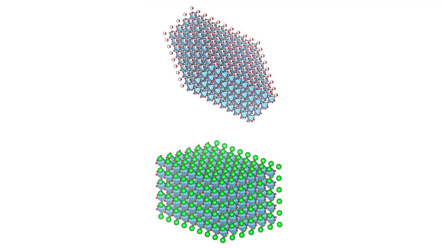
Research from a team led by scientists at the U.S. Department of Energy's (DOE) Argonne National Laboratory offers a new, nanoscopic view of complex oxides, which are promising for advanced microelectronics.
Complex oxides are multifunctional materials that could eventually lead to energy-efficient, advanced electronic memory components and quantum computing devices. Generally, these materials are produced layer-by-layer on an atomically matched substrate, a process known as epitaxial growth.
"Our study shows that this material is ready to go for future microelectronic applications, but it will require further research on ways to avoid these ripples," Saidur Rahman Bakaul, Argonne assistant materials scientist.
To use complex oxides in electronics, they need to be produced on silicon -- an impossible task for existing epitaxial growth techniques, since the atomic structures of these two materials do not match. One possible workaround is to grow the complex oxides elsewhere and then transfer the film to another substrate. However, a key question arises: Will the local properties of a complex oxide thin film remain intact if you lift it from one substrate and deposit it on another?
The new research reveals insights about freestanding complex oxides that could eventually create an entirely new research field: complex oxide microelectronics. The work is detailed in a paper recently published in the journal Advanced Materials.
Using scanning probe microscopy, the team studied lead zirconium titanate (PZT), a type of single-crystal complex oxide ferroelectric thin film. Such single-crystal films have properties ideal for microelectronics: they are highly polarized, endurable and fast-switchable, making them suitable for future ferroelectric random-access memory chips, for example.
Growing these thin films requires temperatures of about 700 °C (1292 °F), which deteriorates the interfacial layer's properties if directly grown on silicon. So the researchers grew the PZT on a more amenable substrate -- a base of strontium titanate (STO) with a "sacrificial layer" of lanthanum strontium manganite (LSMO) sandwiched in between. To transfer the PZT thin film to another substrate, the researchers broke the bonds that united it with the LSMO.
"PZT grows beautifully on LSMO," said Saidur Rahman Bakaul, an assistant materials scientist at Argonne who led the study. "We wanted to see what happens if we cut that interface."
After transforming the PZT into a freestanding film, the research team flipped the film over and gently redeposited it onto an identical STO-LSMO substrate. This allowed for a first-ever view of PZT's detached underside.
"It's like looking at the other side of the moon, which you normally don't see," Bakaul said.
The team used electrostatic force microscopy with 20-nanometer-radius probes to measure the material's local ferroelectric properties. Their analysis showed the local static properties of the bottom surface of freestanding PZT were quite similar compared to those of the top surface. This finding, Bakaul said, is very encouraging for future complex oxide microelectronics, because it confirms that the interfacial surface of the transferred PZT film is a high-quality ferroelectric layer. That means the transfer technique should be able to combine the best materials from different worlds, such as PZT (ferroelectric) and silicon (semiconductors). So far, no direct growth technique has achieved this without damaging the interfacial surface.
Using piezoresponse force microscopy images , scientists found that the detached layer's ferroelectric domain wall velocity -- a measure of the electrostatic energy landscape of complex oxides -- was almost 1,000 times slower than strongly bonded as-grown PZT films.
To find out why, the team first examined the atomic layers at the bottom surface of the PZT film with atomic force microscopy, which revealed anomalies on the surface. For an even closer look, they turned to Argonne's Center for Nanoscale Materials and Advanced Photon Source, both DOE Office of Science User Facilities, to use their joint hard X-ray nanoprobe to see the tilts in atomic planes, revealing never-before-seen ripples.
The ripples, Bakaul said, rise to the height of only a millionth of a pinhead's diameter, but still can create a strong electric field that keeps the domain wall from moving, the theoretical analysis revealed. This claim was further supported with measurements from a scanning capacitance microscope.
The presence of such structural ripples in complex oxides, which used to be known as nonbendable ceramics, is an exciting new scientific discovery and a future playground to explore strong strain gradient-induced physical phenomena such as flexoelectric effects. However, in microelectronic devices, these tiny ripples can induce device-to-device variability.
The work, which was supported by DOE's Office of Basic Energy Sciences, offers a unique and important level of detail about the properties of freestanding complex oxide thin films.
"Our study shows that this material is ready to go for future microelectronic applications," Bakaul said, "but it will require further research on ways to avoid these ripples."
Ferroelectric Domain Wall Motion in Freestanding Single‐Crystal Complex Oxide Thin Film
Saidur R. Bakaul Jaegyu Kim Seungbum Hong Mathew J. Cherukara Tao Zhou Liliana Stan Claudy R. Serrao Sayeef Salahuddin Amanda K. Petford‐Long Dillon D. Fong Martin V. Holt
Advanced Materials 09 December 2019
Contact information:
Assistant Materials Scientist
sbakaul@anl.gov
Phone: (630) 252-1366

Waste polyamide-derived CQDs show continuous photoluminescence tuning from 308 to 552 nm through sequential defect-state engineering, with optical transition energies decreasing from 4.32 to 2.50 eV. @Christian Ebere Enyoh from Saitama University Carbon quantum dots (CQDs) are fluorescent carbon nanomaterials with potential applications in sensing, optoelectronics, displays, anti-counterfeiting, and environmental technologies. Their optical properties can be adjusted by modifying the carbon...

The researchers used circularly polarized light at normal incidence and found that helicity-dependent photocurrents appeared perpendicular to the crystal’s polarization but vanished when measured parallel to it, supporting a bulk origin of CPGE. @Institute of Science Tokyo The circular photogalvanic effect (CPGE), a phenomenon that generates helicity-dependent photocurrents in noncentrosymmetric materials, can originate purely from a crystal's internal structure without contribution from the...

Summary of gold nanoparticle growth programming in liposome based on localization of biomineralization peptide The position of biomineralization peptides within liposomes can influence how gold nanoparticles grow, reports a research team from Institute of Science Tokyo. Peptides localized at the membrane interface promote branched structures, while those confined to the liposome interior favor spherical nanoparticles. The findings offer a new strategy for controlling nanoscale reaction...
