Science China Press
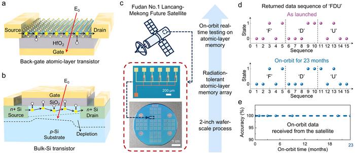
An atomic-layer MoS2 memory array developed at Fudan University has retained its stored data after 23 months in space, with the accuracy of the returned memory data remaining at 100%. Deployed aboard the Fudan No.1 Lancang-Mekong Future Satellite, the array enabled the first demonstration of on-orbit real-time testing of atomic-layer memory. Together with ground irradiation experiments, the results demonstrate the potential of radiation-tolerant, low-noise atomic-layer memory for space applications.
The study, published in National Science Review on November 6, 2026, addresses a key challenge for space exploration: preserving information in a harsh radiation environment. Satellites depend on memory to store essential programs and scientific data. Radiation can introduce defects and trap states into electronic devices, changing their electrical characteristics and making stored information harder to read reliably.
Atomic-layer semiconductors offer a promising approach to this challenge. Their atomically thin functional layers can limit the accumulation of radiation-induced defects. The researchers used monolayer molybdenum disulfide, or MoS2, to fabricate a memory array through a 2-inch wafer-scale process. The device design combines radiation tolerance with low-noise performance, helping maintain a clear distinction between the on and off states.
To investigate its performance in a real space environment, the team deployed the memory aboard the Fudan No.1 Lancang-Mekong Future Satellite. Launched on September 24, 2024, the satellite entered a sun-synchronous low Earth orbit approximately 517 kilometers above Earth. The memory stored the letters ‘FDU’ as 15 binary bits, which were read aboard the satellite and transmitted to a ground station.
After 23 months of on-orbit testing, the returned data remained consistent with the originally programmed information. All reported complete readout records matched the stored message, without error-correction codes, majority voting or additional redundancy. Testing the memory while it operated on orbit provided direct evidence of its performance in space, complementing ground-based irradiation experiments and post-flight laboratory measurements.
In the ground experiments, the researchers exposed the devices to Co-60 γ-ray irradiation at total doses up to 20 Mrad. Measurements on atomic-layer MoS2 transistors showed that their on/off current ratios remained stable after irradiation. The read currents of the on and off states differed by approximately eight orders of magnitude, allowing the two states to remain clearly distinguishable even after high-dose radiation exposure. Besides, based on its radiation tolerance, the nominal on-orbit dose-accumulation time of the atomic-layer MoS2 memory array is expected to be up to 500 years.
The devices also maintained low-noise performance. Electrical noise consists of unwanted signal fluctuations that can interfere with data readout. In particular, low-frequency noise can reduce the signal-to-noise ratio and make it harder to distinguish memory states. Measurements showed that the atomic-layer devices retained their low-noise characteristics even after 20 Mrad γ-ray irradiation. These results support reliable data readout at picoampere current levels.
Led by corresponding author Peng Zhou, the study combines wafer-scale fabrication, ground irradiation experiments and on-orbit real-time testing to demonstrate stable storage and low-noise performance. The findings represent a substantial step toward the practical application of atomic-layer space electronics.
Reference
Spaceborne radiation-tolerant atomic-layer memory with on-orbit real-time testing
Liyuan Zhu, Tanjun Wang, Zhize Lv, Shunli Ma, Yang Yang, Xiaolei Sun, Qiang Zhao, Chunsen Liu, and Peng Zhou
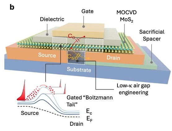
Researchers have fabricated transistors from molybdenum disulfide, an atomically thin two dimensional semiconductor, with channel lengths below five nanometers. An air gap beneath the channel lets the gate keep tighter control of current and curb leakage, delivering switching performance beyond silicon's theoretical limit at comparable size. The devices were built across a four inch wafer, pointing to manufacturability.
TESCAN ORSAY HOLDING, a.s. demonstrated its semiconductor failure analysis workflow at ISTFA 2026, built around Inspect, Access, Prepare and Analyze stages. Conference discussions covered AI-assisted workflows, laser sample preparation and strain analysis.

KAIST researchers developed etching-flux-mediated single-centered nucleation, using oxygen released from a hafnium oxide barrier to suppress molybdenum disulfide nuclei unevenly, so a single crystal forms at a chosen center in over 99% of 400 patterns. Turning nucleation from a random event into a design parameter enables high-quality 2D semiconductors grown directly where needed, supporting stacked AI chips that cut data-movement delays and power consumption.
This week in nanotech
$129.9M raised
6 funding rounds · 39 deals tracked
New products
 Ti-WCMBN Nanomaterialia Featured
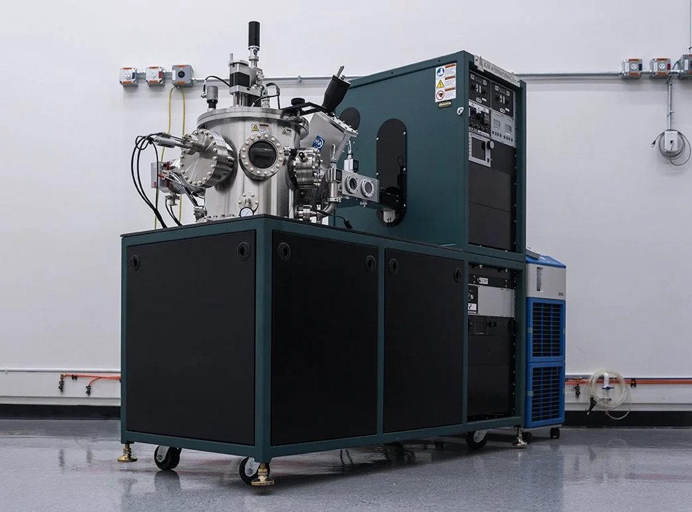 Orion Sputtering Deposition SystemsAJA International Featured
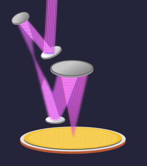 Aether®Lam Research
Market insights
Last 30 days: Semiconductors & Electronics drew the most money: $547.7M.
Money raised per month