16 October 2026. TESCAN ORSAY HOLDING, a.s. participated in ISTFA 2026 and demonstrated its semiconductor failure analysis workflow at Booth 605. The workflow is built around four connected stages: Inspect, Access, Prepare and Analyze.
The workflow combines complementary technologies to support the full failure analysis process, from initial non-destructive inspection through targeted sample preparation and detailed characterization. According to Tescan, connecting each stage lets engineers identify areas of interest, access buried structures, prepare high-quality samples and perform required analyses.
Discussions at the conference focused on electrical and physical fault isolation, device delayering, SEM imaging, TEM sample preparation and the need for higher-throughput analysis workflows. A recurring theme was interest in artificial intelligence and automation, including AI-assisted workflows to reduce analysis time, improve defect localization and support more consistent decision-making.
Tescan reports significant interest in FemtoChisel and discussions around Tescan TENSOR. Presentations included an AI-based end-to-end failure analysis pipeline by Dr. Pouya Tavousi, laser sample preparation and device de-processing by Dave Zapotok, and STEM nanobeam diffraction for strain analysis at sub-2 nm resolution by Dr. Daniel Němeček.
Source: TESCAN ORSAY HOLDING, a.s. news
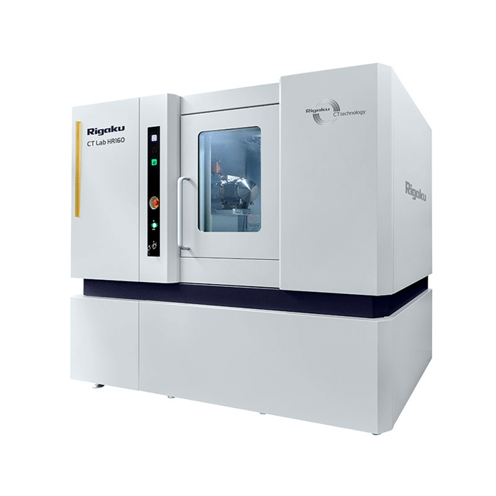
Rigaku has launched the CT Lab HR160, an X-ray CT system combining its imaging expertise with Excillum's NanoTube N3 X-ray source. It operates at up to 160 kV and achieves true 250 nm spatial resolution.
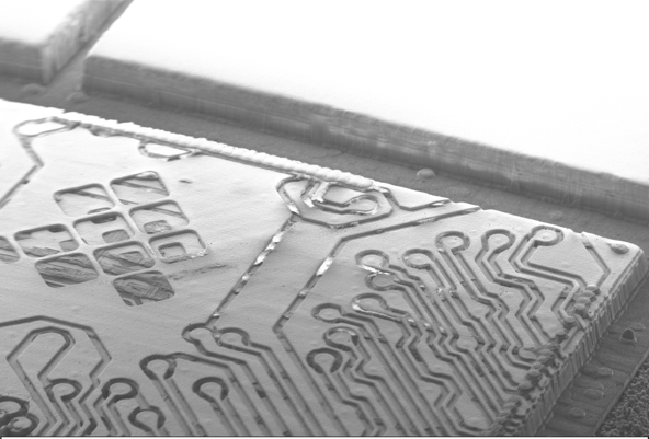
TESCAN ORSAY HOLDING, a.s. has described an A15 semiconductor failure analysis workflow that connects X-ray CT, ultrafast laser processing, optical and confocal microscopy, and SEM for progressive access to buried structures.
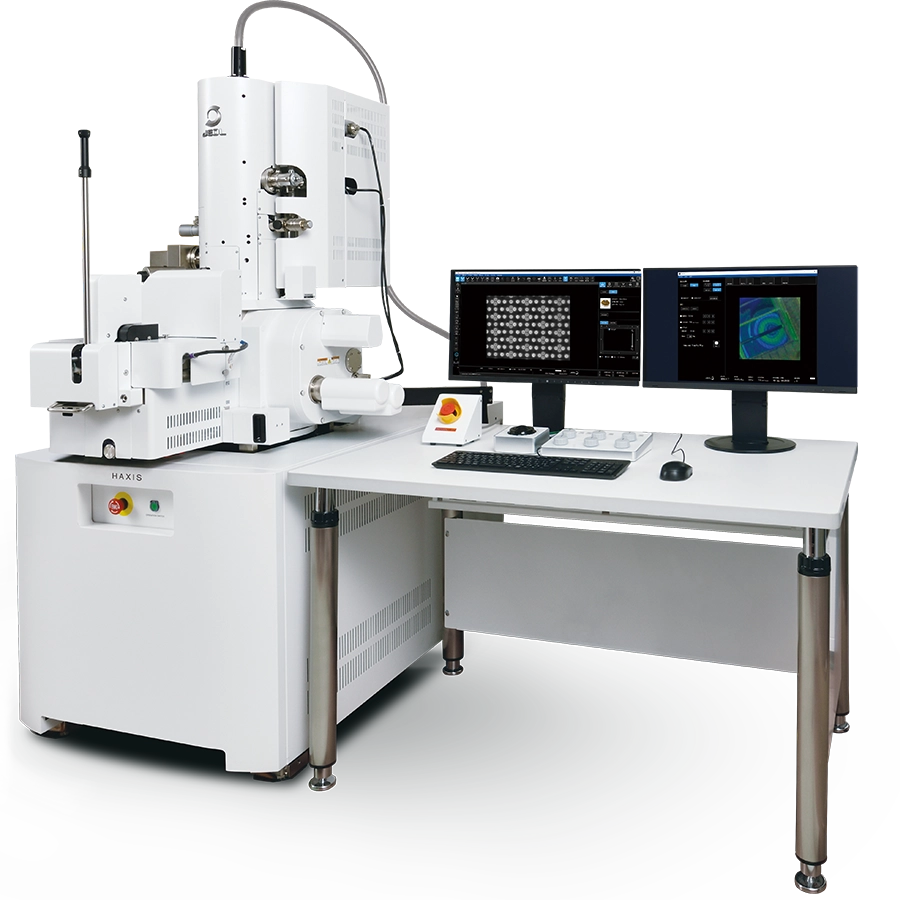
JEOL has started sales of HAXIS, a scanning electron microscope with low-angle argon ion milling and passive voltage contrast detection, for layer-by-layer semiconductor failure analysis.