Malta, N.Y., 14 October 2026. GlobalFoundries (Nasdaq: GFS) has been selected as the technology provider and operator for two new semiconductor manufacturing facilities at its Malta, New York, site under a U.S.-Japan initiative providing up to $21 billion in funding. The initiative follows President Donald J. Trump's trade and investment agreement with Japan.
An initial investment of approximately $10 billion will accelerate construction of a new 300mm semiconductor fab, expected to come online in 2029. An additional investment of approximately $10 billion would fund a second fab. The first fab is expected to add approximately 900,000 300mm wafers of annual U.S. manufacturing capacity when fully operational. A second fab would add approximately the same amount.
The project is expected to create about 27,000 construction and ecosystem jobs and more than 1,000 high-skilled manufacturing jobs in New York's Capital Region. GF expects to break ground on the first fab at its Malta site later this year.
GF has agreed with the U.S. Department of Commerce to amend its existing CHIPS and Science Act award to reallocate $955 million and accelerate investments in silicon photonics, silicon-germanium (SiGe) and advanced packaging at its facilities in Malta, New York, and Burlington, Vermont. In a separate agreement, the U.S. Department of Commerce will receive equity in GF of approximately four percent.
"GF was selected because fabs of this scale require more than capital. They require differentiated technology, operational excellence and a proven ability to execute," said Tim Breen, CEO of GlobalFoundries.
Source: GLOBALFOUNDRIES news
Fraunhofer IZM and Swissbit described Europe's advanced packaging gap between pilot production and mass manufacturing. Fraunhofer's Rolf Aschenbrenner and Swissbit's Lars Lust said low volumes such as 20 to 100 wafers per year are too small for large OSAT providers.
Applied Materials opened its Equipment and Process Innovation and Commercialization (EPIC) Center in Silicon Valley on Oct. 12. The company bets $5 billion on the facility to develop future semiconductor technologies.
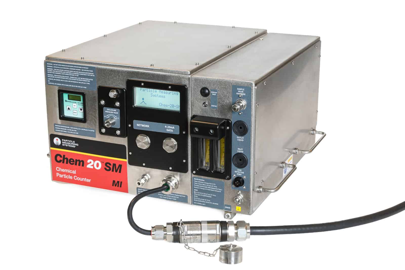
Particle Measuring Systems has launched the Chem 20 SM, a 20 nm solvent particle counter engineered for use in hazardous areas. It monitors solvents such as IPA and PGMEA and is designed to meet IECEx, ATEX and NFPA 70 NEC Class I Division 2 standards.