Munich, 9 November 2026. Infineon Technologies AG has successfully processed 300-millimeter silicon carbide wafers into functional power devices at its fab in Villach, Austria. The company states it is the first to reach this step in a full-scale semiconductor fab environment, using existing silicon manufacturing equipment.
Infineon says chip production on 300 mm wafers is more efficient than on 200 mm wafers, as the larger diameter offers 2.3 times more chips per wafer.
"This technological milestone further strengthens our leadership in power systems. Congratulations and thank you to our passionate team, making significant progress in bringing 300-millimeter SiC out of the lab into a manufacturing environment," said Jochen Hanebeck, CEO of Infineon Technologies.
Infineon will plan the 300-millimeter SiC technology and ramp timing in close collaboration with its customers and partners. The company said it will continue executing its 200-millimeter SiC manufacturing roadmap.
In parallel, Infineon has proofed the feasibility of its Cold Split technology with 300-millimeter SiC at its Dresden, Germany, site. Cold Split separates wafers from a SiC boule with less material loss and reduced processing time compared with conventional wire sawing.
Infineon will show the world's first processed 300-millimeter SiC wafer at electronica in Munich from 10 to 13 November, in Hall C3, Booth 502.
Source: Infineon Technologies AG news
MRDI will lead and operate Hong Kong's first national manufacturing innovation centre, supported by the region's First Five-Year Plan and 2026 Policy Address. The institute is installing two pilot lines for third-generation semiconductor chips at the Yuen Long InnoPark.
Wolfspeed and Infineon expanded and extended their long-term silicon carbide wafer supply agreement. The deal adds 200 mm silicon carbide wafers to the existing 150 mm supply.
Wolfspeed announced a conditional loan commitment letter from the U.S. Department of War for up to $1.5 billion of long-term financing for silicon carbide materials and wide bandgap power devices.
This week in nanotech
10 deals tracked
New products
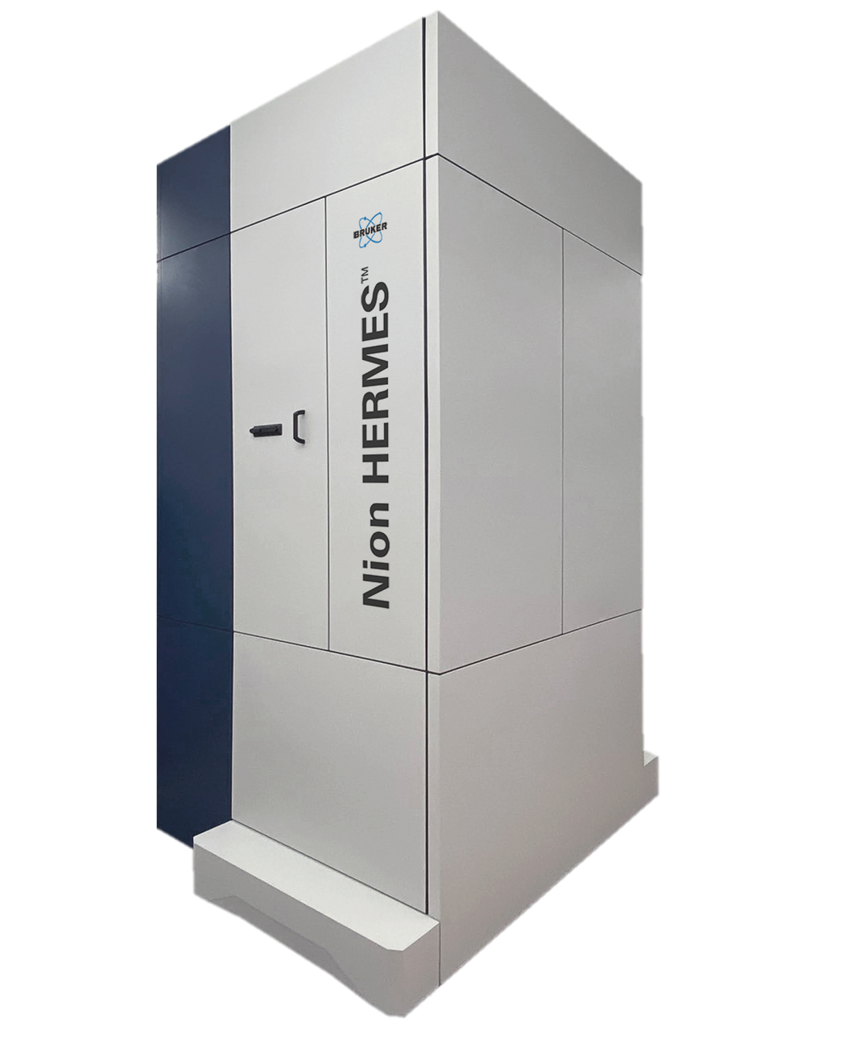 Nion-compatible In Situ STEM Holders for Electrical BiasingHummingbird Scientific Featured
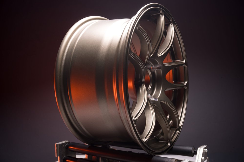 Ti-WCMBN Nanomaterialia Featured
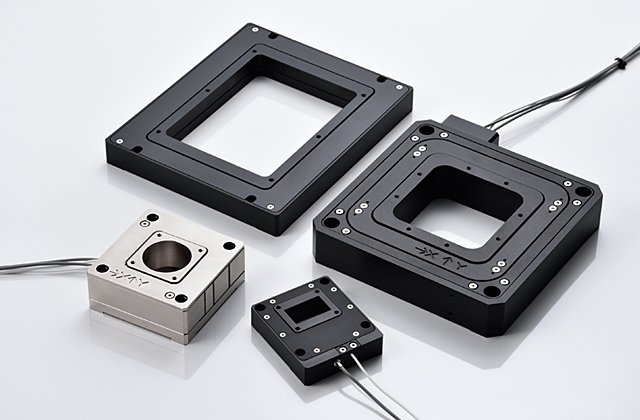 PKVH / PKVL ZAxis With an opening modelTHK PRECISION CO.,LTD.
Market insights
Last 30 days: Semiconductors & Electronics was the busiest vertical: 44 of 142 events (31%).
Money raised per month