19 October 2026. Keysight Technologies Inc of Santa Rosa, CA, USA, via its office in Winnersh, UK, has collaborated with the University of Glasgow, the National Physical Laboratory (NPL) in Teddington, UK, and Taiwan-headquartered MPI Corp to develop a new approach to broadband characterization of next-generation sub-terahertz (sub-THz) semiconductor devices.
The organizations demonstrated continuous on-wafer characterization of indium phosphide high-electron-mobility transistors (InP HEMTs) from near-DC to 250GHz in a single sweep. Keysight says conventional approaches can require multiple measurement setups and calibrations, adding complexity and making consistent data for broadband device modeling more difficult.
The four organizations combined Keysight instrumentation, University of Glasgow semiconductor devices, MPI on-wafer probing technology and NPL metrology expertise. The setup enabled continuous measurement from near-DC to 250GHz with a single probe touchdown. Built-in source filtering and broadband source power calibration helped ensure signal purity at the probe-tip.
Thierry Locquette, VP of sales, Europe, Middle East & Africa at Keysight, said: "Characterizing devices continuously from near-DC to 250GHz in a single sweep can significantly simplify the measurement process for researchers developing next-generation semiconductor technologies."
Dr Xiaobang Shang, principal scientist and on-wafer measurement lead at NPL, said NPL contributed its high-frequency on-wafer metrology and calibration expertise to the collaboration.
Source: Semiconductor Today
HORIBA STEC KOREA will produce the D500 series mass flow controller in Korea, with mass production slated from June 2021 and a target of 1,000 units per month by the end of 2021.
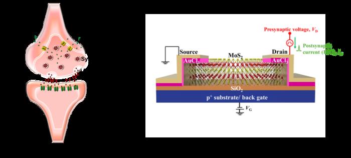
A University of Tokyo team led by Daisuke Kiriya has tuned a planar MoS2 memtransistor by treating its electrical contacts with a solution-based AuCl3 process, leaving the channel largely intact. The treatment raises the effective Schottky barrier from about 40.8 to 196 meV, producing bipolar resistive switching and synaptic behaviors such as long-term potentiation and spike-timing-dependent plasticity.
Allwin21 provides upgrade kits for Branson/IPC L3200 plasma systems, replacing obsolete controllers, electronics and control modules while preserving the original process platform.
This week in nanotech
$110M raised
9 funding rounds · 58 deals tracked
New products
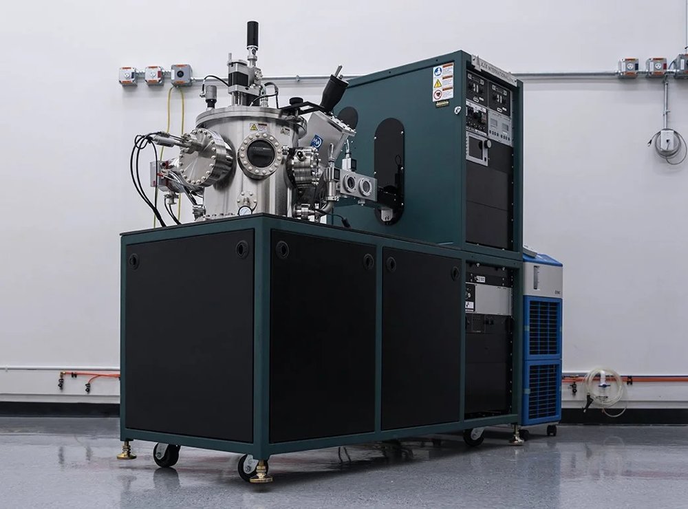 Orion Sputtering Deposition SystemsAJA International Featured
 Ti-WCMBN Nanomaterialia Featured
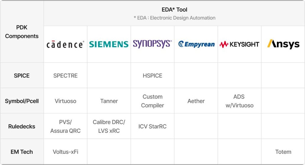 PDK (Process Design Kit)DB HiTek
Market insights
Last 30 days: Quantum Technologies drew the most money: $3.17B.
Money raised per month
Behind the deal
Who led Qilimanjaro Quantum Tech’s $21.9M Series A?
See the investors with Insights Pro →