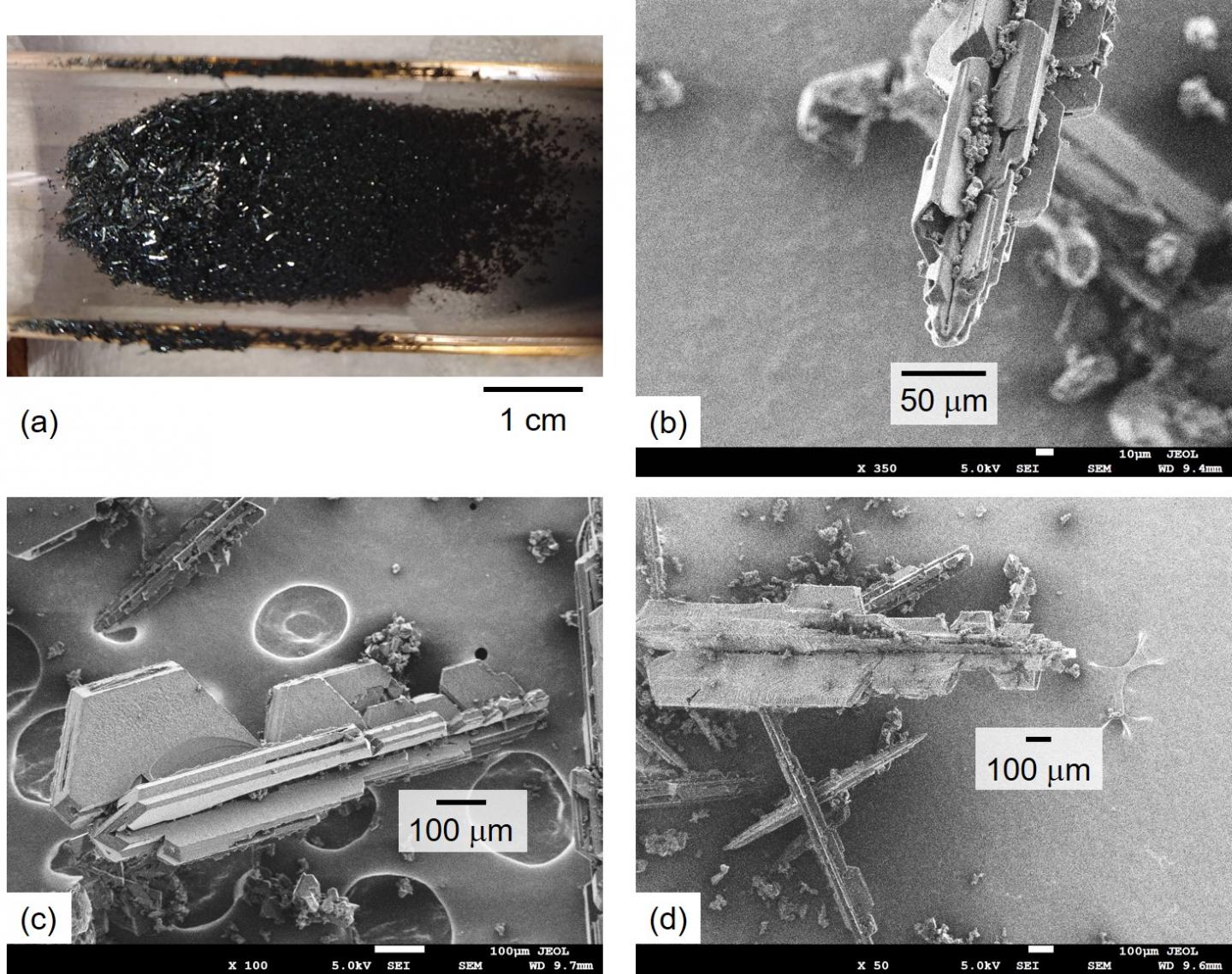
Researchers from Yokohama National University and the University of Electro-Communications in Japan have developed a highly efficient technique for producing a unique fullerene crystal, called fullerene finned-micropillar (FFMP), that is of significant use for next-generation electronics.
Fullerene is a popular choice for developing technologies not only due to its small size, it is also very durable and contains semiconductor properties, making it a good candidate in devices such as field-effect transistors, solar cells, superconductive materials, and chemical sensors. The material is in use now, however, it is difficult to handle because fullerene is a nano-scaled and generally come in a powdery state. As a solution of this problem, one-dimensional fullerene crystals are produced and used.
"Producing one-dimensional fullerene crystals requires expert skills and takes several days with typical production methods. In this study, we succeeded in developing a very simple fabricating method by using an annealing process," said Dr. Takahide Oya, Associate Professor at Yokohama National University and corresponding author of the study.
In a paper published in Scientific Reports in November 2020 (DOI: 10.1038/s41598-020-76252-6), the team details how they utilized a small heating apparatus that accepted fullerene and heated it to a temperature of 1,173 Kelvin for about an hour. The fullerene originally deposited in the heating apparatus de-crystallizes due to the heat and subsequently re-crystallizes as the temperature is lowered. This overall process, known as annealing, is over fifty times faster than the older technique for producing fullerene crystals.
"By using our method, mass production of one-dimensional fullerene crystals can be produced in an hour. The produced fullerene crystals that we named 'fullerene finned-micropillar (FFMP)' have a distinctive structure," said Oya.
The team is also confident that the fullerene crystals produced in this new, more efficient production process will have similar qualities to fullerene crystals such as fullerene nanowhiskers produced using the older methods.
"FFMP is expected to have electrical conductivity and n-type semiconductor functionality," Oya said.
More tests are required to confirm that FFMP does indeed retain the qualities so useful for electronic implementation, but positive results could mean solar cells with much higher efficiency, extremely small circuits integrated in flexible devices for example.
The team has already examined this annealing under different environmental conditions, temperatures, and heating time. Having studied the process, the team now has their sights set on characterizing the FFMP in the context of an electrical component. "As the next step of this study, confirming and obtaining the electrical conductivity and the n-type semiconductor functionality is expected, because the ordinary fullerene has such properties. In addition, developing 'fullerene-finned nano pillar (FFNP)' by modifying the process is also expected. We believe that FFMPs (or FFNPs) will be useful for field-effect transistors, organic photovoltaics, and so on in the near future," said Oya.
This will not be the first time Oya and his team have tackled special, small scale materials for use in electronics.
"We have already had a technique for making carbon nanotube, or CNT -- one dimensional nano-carbon material -- composite papers and CNT composite threads/textiles as unique CNT composite materials," said Oya. "Therefore, we will develop FFMP composite materials along with their applications. We believe the useful FFMP composites (and the combination with CNT composites) will be used in our daily life in near future."
Contact
Takahide Oya
Graduate School of Engineering Science
Yokohama National University
oya-takahide-vx@ynu.ac.jp
Reference
Simple annealing process for producing unique one-dimensional fullerene crystal named fullerene finned-micropillar
Taku Onishi, Takahiro Tsukamoto & Takahide Oya
