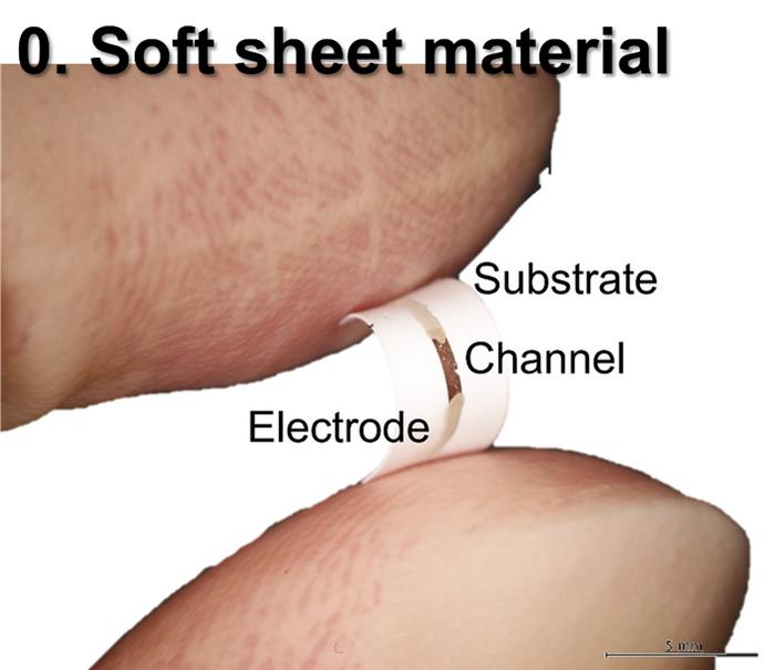
Led by Assistant Professor Kou Li, a research group in Chuo University, Japan, has developed chemically enriched photo-thermoelectric (PTE) imagers using semiconducting carbon nanotube (CNT) films, resulting in the achievement of enhanced response intensity and noise reduction, that enables efficient remote and on-site inspections, according to a recent paper publication in Communications Materials. CNT film-based PTE imagers are crucial for multimodal non-destructive inspection, but conventional device design strategies have faced challenges in achieving high response intensity for wireless data logging.
CNT film-based PTE imagers enable functional electromagnetic-wave monitoring, potentially facilitating multimodal non-destructive inspection device usage. The CNT film compositions govern the fundamental device performance, and satisfying high PTE conversion efficiency (higher response and lower noise) is essential for sensitive operations. Although typical sensitive design focuses on minimising noise, the associated levelling-off response intensity (up to a few millivolts) induces technical limitations in device operations. These issues include mismatching for coupling with compact wireless circuits, which are indispensable for on-site inspection applications and require high-intensity responses at least a few millivolt orders. This work develops chemically enriched PTE imagers comprising semiconducting CNT (semi-CNT) films. While semi-CNTs provide greater intensity thermoelectric responses than semi-metal mixture compositions in the conventional PTE device, the presented imager employs p-/n-type chemical carrier doping to relax inherent significant bottlenecking noise. Such doping enhances material properties for PTE conversion with semi-CNTs up to 4,060 times. The imager satisfies similar performances to conventional CNT film devices, including ultrabroadband sensitive photo-detection (with minimum noise sensitivity of 5 pWHz−1/2) under repeatedly deformable configurations, and advantageously exhibits response signal intensity exceeding a few–tens of millivolts. These features enable remote on-site non-destructive PTE imaging inspection with palm-sized wireless circuits.
Research background
While quality testing techniques are essential in rapidly growing industrial mass-production and social distribution, optically broadband and mechanically deformable photo image sensors (photo-imagers) potentially play a leading role in non-destructive inspection by handling diverse target objects. However, such the existing photo-imagers still function with low (from tens to hundreds of microvolts) intensity responses, limiting choices of system setups. These crucial bottlenecks include mismatching for operating the above devices with compact wireless datalogger circuits (available in millivolt (mV) orders), which are essential in non-destructive inspection regarding on-site use. Furthermore, due to levelling-off response intensities, the conventional device design has mainly focused on minimising noise signals for sensitivity enhancements, which are off the point for satisfying technical requirements for the above remote operations. These situations hinder the broadband deformable photo-imagers from their versatile applications.
The importance and novelty of this work
To this end, this work made the following significant contributions.
Reference
A chemically enriched, repeatedly deformable, and self-recoverable broadband wireless imager sheet
Kou Li, Norika Takahashi, Yoshiaki Togami, Ryo Koshimizu, Noa Izumi, Naoko Hagiwara, Asumi Sano, Qi Zhang, Junyu Jin, Minami Yamamoto & Yukio Kawano
https://www.nature.com/articles/s43246-025-00872-6
Chuo University
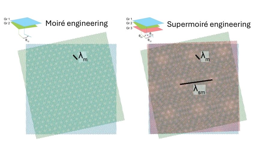
Stacking and twisting two graphene layers forms a moiré pattern, enabling superconductivity. Adding a third, differently twisted layer creates supermoiré patterns, altering electron flow. Harvard SEAS researchers, led by Yonglong Xie and Andrew Pierce, used a 100-nanometer resolution microscope to probe trilayer graphene. Published in Science, their findings reveal novel electronic states, highlighting supermoiré patterns’ role in engineering tunable materials for quantum tech and electronics.
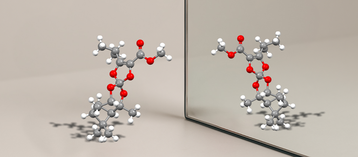
A team from UNIGE and the University of Pisa has designed surprisingly stable molecular assemblies, paving the way for new drug constructs and geometrically controlled materials.

The chip, as thin as a strand of hair, uses two pairs of microring modulators to achieve unprecedented performance levels.
This week in nanotech
$271M raised
6 funding rounds · 27 deals tracked
New products
 Ti-WCMBN Nanomaterialia Featured
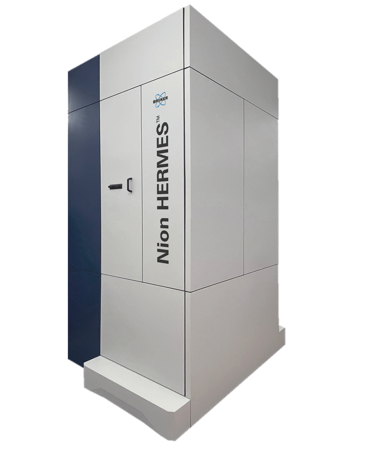 Nion-compatible In Situ STEM Holders for Electrical BiasingHummingbird Scientific Featured
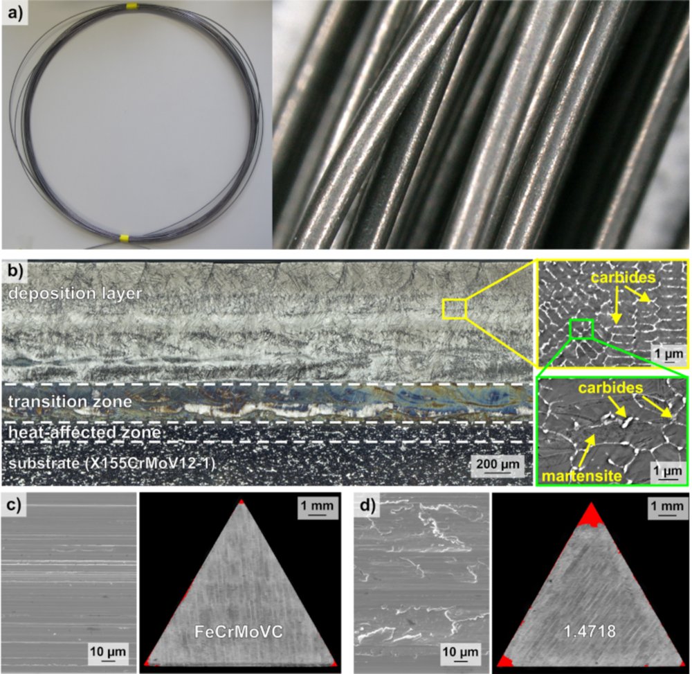 Fe85Cr4Mo8V2C1 wire filler materialLeibniz Institute for Solid State and Materials Research Dresden - IFW Dresden
Market insights
Last 30 days: Quantum Technologies drew the most money: $3.17B.
Money raised per month
Behind the deal
Who led Xanadu Quantum Technologies Limited’s $10M Grant?
See the investors with Insights Pro →