Scientists from The University of Manchester have developed a novel yet simple method for producing vertical stacks of alternating superconductor and insulator layers of tantalum disulphide (TaS2). The findings, from a team led by Professor Rahul Nair, could speed up the process of manufacturing such devices – so-called van der Waals heterostructures – with application in high-mobility transistors, photovoltaics and optoelectronics.
Van der Waals heterostructures are much sought after since they display many unique and useful properties not found in naturally occurring materials. In most cases, they are prepared by manually stacking one layer over the other in a time-consuming and labour-intensive process.
Published last week in the journal Nano Letters, the study - led by researchers based at the National Graphene Institute (NGI) - describes synthesis of a bulk van der Waals heterostructure consisting of alternating atomic layers of 1T and 1H TaS2. 1T and 1H TaS2 are different polymorphs (materials with the same chemical composition but with a variation in atomic arrangement) of TaS2 with completely different properties – the former insulating, the latter superconducting at low temperatures.
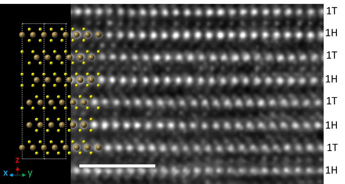
The new heterostructure was obtained through the synthesis of 6R TaS2 (a rare type of TaS2, with alternating 1T and 1H layered structure) via a process known as ‘phase transition’ at high temperature (800˚C). Due to its unusual structure, this material shows the co-existence of superconductivity and charge density waves, a very rare phenomenon.
Dr Amritroop Achari, who led the experiment said: “Our work presents a new concept for designing bulk heterostructures. The novel methodology allows the direct synthesis of bulk heterostructures of 1T‐1H TaS2 by a phase transition from a readily available 1T TaS2. We believe our work provides significant advances in both science and technology.”
International collaboration
The work was conducted in collaboration with scientists from the NANOlab Center of Excellence at the University of Antwerp, Belgium. Their high‐resolution scanning electron microscopy analysis unambiguously proved the alternating 1T‐1H hetero-layered structure of 6R TaS2 for the first time and paved the way to interpret the findings.
Professor Milorad Milošević, the lead researcher from the University of Antwerp, commented: “This demonstration of an alternating insulating‐superconducting layered structure in 6R TaS2 opens a plethora of intriguing questions related to anisotropic behaviour of this material in applied magnetic field and current, emergent Josephson physics, terahertz emission etc., in analogy to bulk cuprates and iron‐based superconductors.”
The findings could therefore have a widespread impact on the understanding of 2D superconductivity, as well as further design of advanced materials for terahertz and Josephson junctions-based devices, a cornerstone of second-generation quantum technology.
Reference
Alternating Superconducting and Charge Density Wave Monolayers within Bulk 6R-TaS2
Amritroop Achari, Jonas Bekaert, Vishnu Sreepal, Andrey Orekhov, Piranavan Kumaravadivel, Minsoo Kim, Nicolas Gauquelin, Premlal Balakrishna Pillai, Johan Verbeeck, Francois M. Peeters, Andre K. Geim, Milorad V. Milošević, and Rahul R. Nair

Waste polyamide-derived CQDs show continuous photoluminescence tuning from 308 to 552 nm through sequential defect-state engineering, with optical transition energies decreasing from 4.32 to 2.50 eV. @Christian Ebere Enyoh from Saitama University Carbon quantum dots (CQDs) are fluorescent carbon nanomaterials with potential applications in sensing, optoelectronics, displays, anti-counterfeiting, and environmental technologies. Their optical properties can be adjusted by modifying the carbon...

The researchers used circularly polarized light at normal incidence and found that helicity-dependent photocurrents appeared perpendicular to the crystal’s polarization but vanished when measured parallel to it, supporting a bulk origin of CPGE. @Institute of Science Tokyo The circular photogalvanic effect (CPGE), a phenomenon that generates helicity-dependent photocurrents in noncentrosymmetric materials, can originate purely from a crystal's internal structure without contribution from the...

Summary of gold nanoparticle growth programming in liposome based on localization of biomineralization peptide The position of biomineralization peptides within liposomes can influence how gold nanoparticles grow, reports a research team from Institute of Science Tokyo. Peptides localized at the membrane interface promote branched structures, while those confined to the liposome interior favor spherical nanoparticles. The findings offer a new strategy for controlling nanoscale reaction...
