Agency for Science, Technology and Research
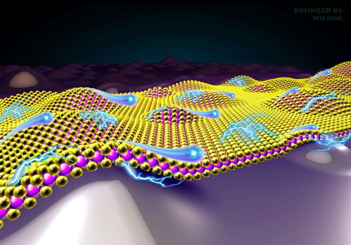
Two dimensional (2D) semiconductors have a unique property that allows their thickness to be reduced to one or few atoms – and this property could potentially minimise the short channel effects that remain an issue in advanced silicon-based transistors, for example, turning on a transistor prematurely.
Despite the potential that 2D semiconductors possess in replacing conventional semiconducting materials like silicon in future, one key challenge remains: their low carrier mobility at room temperature, caused by strong scattering between electrons and phonons.
Road and traffic conditions determine the amount of time and energy that a person spends travelling from one location to another. In a similar fashion, carrier mobility measures how quickly a carrier, such as an electron or a hole, can move through a material when there is an electric field. This characteristic also determines whether a semiconducting material is suitable for electronic devices.
High carrier mobility can effectively reduce power dissipation in integrated circuits and lower the overall power consumption, thus prolonging the lifetime of electric devices or systems, as well as reducing the costs of running these devices or systems.
Researchers from the Agency for Science, Technology and Research’s (A*STAR) Institute of Materials Research and Engineering (IMRE), Fudan University, National University of Singapore and The Hong Kong Polytechnic University have recently found that placing 2D materials on substrates with bulged morphologies can enhance carrier mobility at room temperature by two orders. These bulges create ripples in the material, thus distorting its lattice structure – moving one or more atoms from their original position in an ideal structure.
This approach contrasts conventional strategies which rely on perfect lattice structures to enhance carrier mobility, as any form of impurity or lattice distortion is regarded to adversely affect mobility.
In a study published in Nature Electronics in June 2022, researchers observed that rippled 2D molybdenum disulfide (MoS2) with lattice distortions create a larger electric polarisation that can renormalise the frequency of phonons. This renormalised phonon frequency effectively reduces the strength of scattering between electrons and phonons, thus increasing carrier mobility in MoS2. This means that electrons can now move faster through the material.
Study results show that carrier mobility at room temperature is enhanced by two orders in rippled MoS2, reaching approximately 900 cm2 V-1 s-1. The observed result exceeds the predicted phonon-limited carrier mobility of flat MoS2 of 200–410 cm2 V-1 s-1.
Through the study, creating bulges in the lattice structure of MoS2 was found to overcome the intrinsic carrier mobility limit of the material. This paves the way for MoS2 and other 2D materials to be used in creating field-effect transistors and thermoelectric devices with competitive performance at room temperature.
“Our approach is simple and cost-effective, demonstrating lattice engineering as an effective strategy to create high-performance room-temperature electronics and thermoelectric devices for future electronics,” said Dr Wu Jing, Scientist at A*STAR’s IMRE.
“We further reveal the underlying mechanism that the improved carrier mobility is due to the suppressed electron-phonon scattering and increased intrinsic dielectric constant induced by the rippled structures in the 2D semiconductor. Both of them play synergistic effects to boost the intrinsic carrier mobility,” said Dr Yang Ming, Assistant Professor at the Department of Applied Physics, The Hong Kong Polytechnic University.
Reference
Improving carrier mobility in two-dimensional semiconductors with rippled materials
Hong Kuan Ng, Du Xiang, Ady Suwardi, Guangwei Hu, Ke Yang, Yunshan Zhao, Tao Liu, Zhonghan Cao, Huajun Liu, Shisheng Li, Jing Cao, Qiang Zhu, Zhaogang Dong, Chee Kiang Ivan Tan, Dongzhi Chi, Cheng-Wei Qiu, Kedar Hippalgaonkar, Goki Eda, Ming Yang & Jing Wu

Waste polyamide-derived CQDs show continuous photoluminescence tuning from 308 to 552 nm through sequential defect-state engineering, with optical transition energies decreasing from 4.32 to 2.50 eV. @Christian Ebere Enyoh from Saitama University Carbon quantum dots (CQDs) are fluorescent carbon nanomaterials with potential applications in sensing, optoelectronics, displays, anti-counterfeiting, and environmental technologies. Their optical properties can be adjusted by modifying the carbon...

The researchers used circularly polarized light at normal incidence and found that helicity-dependent photocurrents appeared perpendicular to the crystal’s polarization but vanished when measured parallel to it, supporting a bulk origin of CPGE. @Institute of Science Tokyo The circular photogalvanic effect (CPGE), a phenomenon that generates helicity-dependent photocurrents in noncentrosymmetric materials, can originate purely from a crystal's internal structure without contribution from the...

Summary of gold nanoparticle growth programming in liposome based on localization of biomineralization peptide The position of biomineralization peptides within liposomes can influence how gold nanoparticles grow, reports a research team from Institute of Science Tokyo. Peptides localized at the membrane interface promote branched structures, while those confined to the liposome interior favor spherical nanoparticles. The findings offer a new strategy for controlling nanoscale reaction...
