Striped or checkered? Magnetic field influences competing electronic patterns in a graphene-like quantum material

Researchers reveal how electronic patterns emerge and can be controlled in the graphene-like quantum material CeTe₃
In most everyday materials, such as copper, silver, and silicon, the behavior of electrons is relatively predictable. In quantum materials, however, electrons can interact in complex ways, giving rise to collective electronic states with remarkable properties. Understanding how these states emerge — and, ultimately, how to control them — is one of the central challenges in quantum materials research.
Now, researchers from the Okinawa Institute of Science and Technology (OIST) and Hiroshima University have discovered that a small magnetic field switches the layered quantum material CeTe₃ between competing electronic states that appear as striped or checkerboard patterns. Published July 23 in Nature Communications, the work reveals how magnetism can reorganize a quantum material’s entire electronic state.

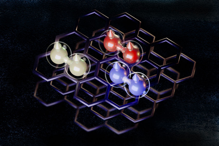
CeTe₃, a material formed from cerium and tellurium atoms, has some similar properties to graphene, in that it is a two-dimensional layered material with highly mobile electrons. But unlike graphene, electrons on the cerium sites remain localized while the mobile electrons on the tellurium sites naturally self-organize into ordered patterns. Thanks to a quantum property called spin, the localized electrons behave like tiny magnets, allowing CeTe3’s electronic states to be manipulated with a magnetic field. Until now, however, no one had directly observed how magnetism influences the evolution of these electronic patterns.
“CeTe₃ offers a rare opportunity to watch mobile electrons and localized spins work together,” says co-first author Yuita Fujisawa, an assistant professor at Hiroshima University and a former postdoctoral researcher in the Quantum Materials Science Unit at OIST, led by Professor Yoshinori Okada. “We wanted to directly visualize how this cooperation gives rise to collective electronic states.”
From stripes to checkerboards
To begin, the researchers used scanning tunneling microscopy (STM) to map how electrons are arranged within CeTe₃ at the atomic scale. Once cooled to near absolute zero, the researchers observed a striped electronic pattern. When they then applied a magnetic field, the striped electronic pattern transformed into a checkerboard pattern.
“I immediately went to Professor Okada's office and said, ‘Look at this!’” recalls Fujisawa. “We were astonished because it is extremely rare for a material to host multiple competing electronic patterns that can be switched so dramatically by such a small magnetic field.”
So why can the material adopt such different electronic patterns so easily? The answer lies in a phenomenon physicists call frustration. In CeTe₃, the electrons can organize themselves into several different low-energy patterns, with no single arrangement preferred.
"Imagine placing a ball on a landscape with several nearly identical valleys," Fujisawa explains. "A slight tilt is enough to make the ball roll into a different valley. In CeTe₃, the magnetic field provides that push, shifting the balance between competing electronic states and switching the material from a striped to a checkerboard pattern.”
Linking magnetic and electronic structures
After discovering the competing electronic patterns, the researchers next sought to understand the kind of magnetic structure underlying them. A second research team, including scientists from OIST, Hiroshima University, the University of Tokyo, the University of the Ryukyus and the High Energy Accelerator Research Organization (KEK), investigated the magnetic structure of CeTe₃ using neutron scattering, a technique capable of directly revealing the arrangement of magnetic moments. Published on the same day in Physical Review B, the complementary study showed that the magnetic order of CeTe₃ becomes unexpectedly complex at temperatures near absolute zero.
“CeTe₃ is antiferromagnetic, which usually means that neighboring spins point in opposite directions. But in this case, we found that the magnetic moments form a much more intricate repeating pattern,” says Ryutaro Okuma, an assistant professor at the University of Tokyo and former postdoctoral researcher at OIST.

Remarkably, this magnetic structure’s periodicity — the length over which the pattern repeats — is proportionate to the striped electronic state observed by STM, providing strong evidence that the magnetic and electronic structures of CeTe₃ are closely linked.
"Our work shows that electronic frustration can be harnessed," says Fujisawa. "By coupling it to magnetism, we can manipulate collective electronic states with a small magnetic field."
Overall, their findings suggest that electronic frustration creates multiple competing electronic states, while magnetism provides a practical way to select between them.
“Harnessing this interplay could offer a new strategy for controlling collective electronic states in materials where these two ingredients coexist,” Fujisawa concludes. “This approach may open new opportunities for future quantum and spintronic technologies, and also could inspire new ways to control competing electronic phases in emerging quantum materials.”
Reference
Versatile electronic phases enabled by intertwined multiple frustrations in an antiferromagnetic two-dimensional semimetal
Y. Fujisawa, P. Wu, T. Nakamura, R. Okuma, T. Kato, B. R. M. Smith, D. Ueta, R. Kobayashi, N. Maekawa, C-H. Hsu, C. De, N. Tomoda, T. Higashihara, K. Morishita, K. Sumida, K. Miyamoto, T. Okuda, Z. Y. Wang & Y. Okada
Nature Communications volume 17, Article number: 5981 (2026)
Okinawa Institute of Science and Technology (OIST) Graduate University