At first glance, mica is something quite ordinary: it is a common mineral, found in granite for example, and has been extensively studied from geological, chemical and technical perspectives.
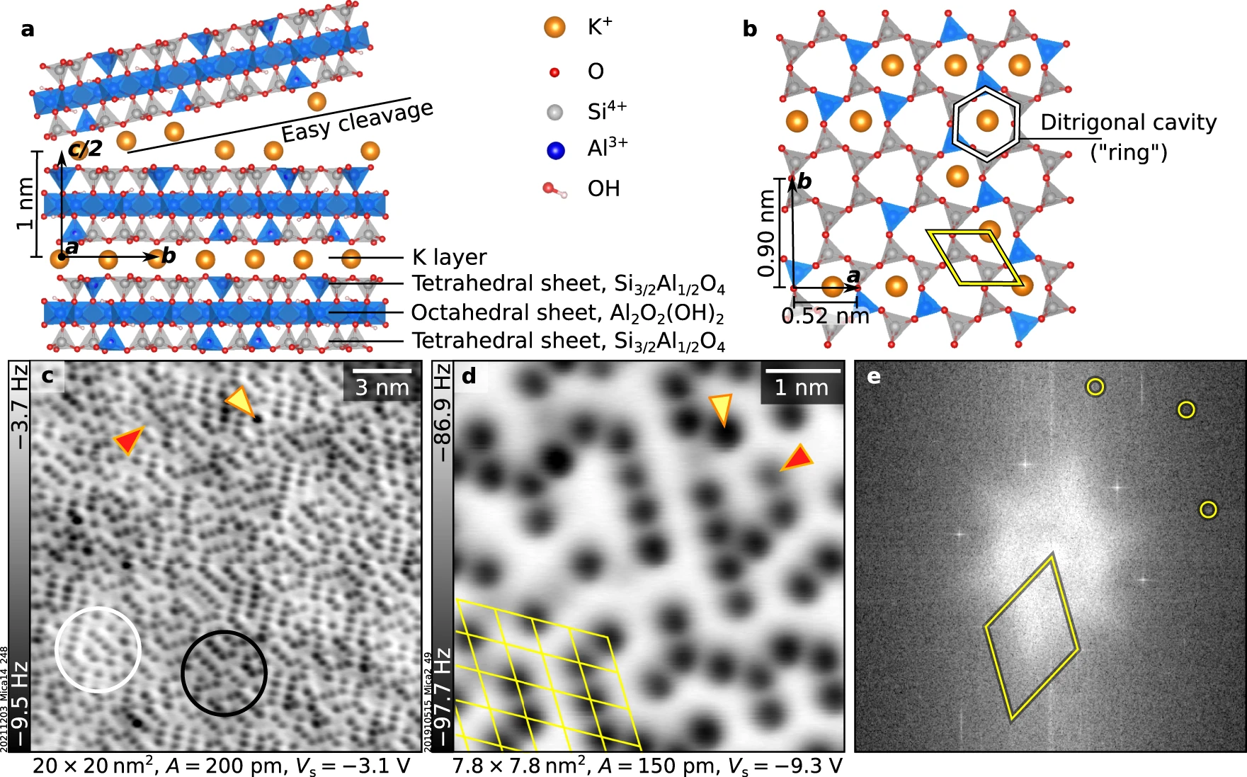
One might think that nothing new can be discovered from such an everyday material. But now a team from the Vienna University of Technology has presented a study in the journal "Nature Communications", in which it was possible to explain the distribution of potassium ions on the mica surface. The physical surface details of mica have never been studied on an atomic scale, and this information is important for research on electronics with 2D materials.
Atomically thin layers
Atomically thin layers 2D materials are currently one of the most researched topics in materials science: Certain materials, such as graphene and molybdenum disulfide, consist of only one or a few layers of atoms, which frequently leads to unusual properties.
In a sense, mica is a naturally occurring 2D material: It consists of atomically thin layers that can contain different atoms depending on the type of mica: oxygen is always present, often silicon, often potassium or aluminum as well. The layer structure of the mica is also the reason for its characteristic sheen - you can often see a spectrum of colors, similar to a thin layer of oil on a puddle of water.
Potassium ions in ultra high vacuum
The outermost layer of mica is difficult to examine because it is quickly contaminated by atoms and molecules from the air. It has now been possible to image the surface of mica in ultra-high vacuum, however, using a new type of atomic force microscope at the Vienna University of Technology. "We were able to see how the potassium ions are distributed on the surface," says Giada Franceschi, the first author of the current paper, who works in Prof. Ulrike Diebold's team. "We were also able to gain insights into the positions of the aluminum ions under the surface layer - this is a particularly difficult task experimentally."
The images from the Vienna University of Technology show that the potassium ions are not randomly distributed on the surface, as previously assumed, but are arranged in tiny patterns. These distributions could also be calculated with the help of computer simulations.
Matching insulator for 2D electronics
This work could be important, among other things, for attempts to use 2D materials such as graphene for electronic circuits. One also needs suitable insulators for this – and mica is a very obvious candidate. “The surface properties of mica will play a crucial role in such electronic components,” says Giada Franceschi.
Reference
Resolving the intrinsic short-range ordering of K+ ions on cleaved muscovite mica
Giada Franceschi, Pavel Kocán, Andrea Conti, Sebastian Brandstetter, Jan Balajka, Igor Sokolović, Markus Valtiner, Florian Mittendorfer, Michael Schmid, Martin Setvín & Ulrike Diebold

Waste polyamide-derived CQDs show continuous photoluminescence tuning from 308 to 552 nm through sequential defect-state engineering, with optical transition energies decreasing from 4.32 to 2.50 eV. @Christian Ebere Enyoh from Saitama University Carbon quantum dots (CQDs) are fluorescent carbon nanomaterials with potential applications in sensing, optoelectronics, displays, anti-counterfeiting, and environmental technologies. Their optical properties can be adjusted by modifying the carbon...

The researchers used circularly polarized light at normal incidence and found that helicity-dependent photocurrents appeared perpendicular to the crystal’s polarization but vanished when measured parallel to it, supporting a bulk origin of CPGE. @Institute of Science Tokyo The circular photogalvanic effect (CPGE), a phenomenon that generates helicity-dependent photocurrents in noncentrosymmetric materials, can originate purely from a crystal's internal structure without contribution from the...

Summary of gold nanoparticle growth programming in liposome based on localization of biomineralization peptide The position of biomineralization peptides within liposomes can influence how gold nanoparticles grow, reports a research team from Institute of Science Tokyo. Peptides localized at the membrane interface promote branched structures, while those confined to the liposome interior favor spherical nanoparticles. The findings offer a new strategy for controlling nanoscale reaction...
