DOE's Berkeley Lab
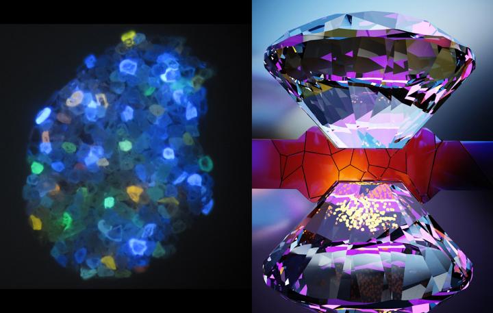
Since their invention more than 60 years ago, diamond anvil cells have made it possible for scientists to recreate extreme phenomena - such as the crushing pressures deep inside the Earth's mantle - or to enable chemical reactions that can only be triggered by intense pressure, all within the confines of a laboratory apparatus that you can safely hold in the palm of your hand.
To develop new, high-performance materials, scientists need to understand how useful properties, such as magnetism and strength, change under such harsh conditions. But often, measuring these properties with enough sensitivity requires a sensor that can withstand the crushing forces inside a diamond anvil cell.
Since 2018, scientists at the Center for Novel Pathways to Quantum Coherence in Materials (NPQC), an Energy Frontier Research Center led by the U.S. Department of Energy's Lawrence Berkeley National Laboratory (Berkeley Lab), have sought to understand how the properties of electronic and optical materials can be harnessed to develop ultrasensitive sensors capable of measuring electric and magnetic fields.
Now, a team of scientists led by Berkeley Lab and UC Berkeley, with support from the NPQC, have come up with a clever solution: By turning natural atomic flaws inside the diamond anvils into tiny quantum sensors, the scientists have developed a tool that opens the door to a wide range of experiments inaccessible to conventional sensors. Their findings, which were reported in the journal Science, have implications for a new generation of smart, designer materials, as well as the synthesis of new chemical compounds, atomically fine-tuned by pressure.
Turning atomic flaws into sensors
At the atomic level, diamonds owe their sturdiness to carbon atoms bound together in a tetrahedral crystal structure. But when diamonds form, some carbon atoms can get bumped out of their "lattice site," a space in the crystal structure that is like their assigned parking spot. When a nitrogen atom impurity trapped in the crystal sits adjacent to an empty site, a special atomic defect forms: a nitrogen-vacancy (NV) center.
Over the last decade, scientists have used NV centers as tiny sensors to measure the magnetism of a single protein, the electric field from a single electron, and the temperature inside a living cell, explained Norman Yao, faculty scientist in Berkeley Lab's Materials Sciences Division and assistant professor of physics at UC Berkeley.
To take advantage of the NV centers' intrinsic sensing properties, Yao and colleagues engineered a thin layer of them directly inside the diamond anvil in order to take a snapshot of the physics within the high-pressure chamber.
Imaging stress inside the diamond anvil cell
After generating a layer of NV center sensors a few hundred atoms in thickness inside one-tenth-carat diamonds, the researchers tested the NV sensors' ability to measure the diamond anvil cell's high-pressure chamber.
The sensors glow a brilliant shade of red when excited with laser light; by probing the brightness of this fluorescence, the researchers were able to see how the sensors responded to small changes in their environment.
What they found surprised them: The NV sensors suggested that the once-flat surface of the diamond anvil began to curve in the center under pressure.
Co-author Raymond Jeanloz, professor of earth and planetary science at UC Berkeley, and his team identified the phenomenon as "cupping" - a concentration of the pressure toward the center of the anvil tips.
"They had known about this effect for decades but were accustomed to seeing it at 20 times the pressure, where you can see the curvature by eye," Yao said. "Remarkably, our diamond anvil sensor was able to detect this tiny curvature at even the lowest pressures."
There were other surprises, too. When a methanol/ethanol mixture they squeezed underwent a glass transition from a liquid to a solid, the diamond surface turned from a smooth bowl to a jagged, textured surface. Mechanical simulations performed by co-author Valery Levitas of Iowa State University and Ames Laboratory confirmed the result.
"This is a fundamentally new way to measure phase transitions in materials at high pressure, and we hope this can complement conventional methods that utilize powerful X-ray radiation from a synchrotron source," said lead author Satcher Hsieh, a doctoral researcher in Berkeley Lab's Materials Sciences Division and in the Yao Group at UC Berkeley.
Co-lead authors with Hsieh are graduate student researcher Prabudhya Bhattacharyya and postdoctoral researcher Chong Zu of the Yao Group at UC Berkeley.
Magnetism under pressure
In another experiment, the researchers used their array of NV sensors to capture a magnetic "snapshot" of iron and gadolinium.
Iron and gadolinium are magnetic metals. Scientists have long known that compressing iron and gadolinium can alter them from a magnetic phase to a nonmagnetic phase, an outcome of what scientists call a "pressure-induced phase transition." In the case of iron, the researchers directly imaged this transition by measuring the depletion of the magnetic field generated by a micron-size (or one millionth of a meter) bead of iron inside the high-pressure chamber.
In the case of gadolinium, the researchers took a different approach. In particular, the electrons inside gadolinium "happily whiz around in random directions," and this chaotic "mosh pit" of electrons generates a fluctuating magnetic field that the NV sensor can measure, Hsieh said.
The researchers noted that the NV center sensors can flip into different magnetic quantum states in the presence of magnetic fluctuations, much like how a compass needle spins in different directions when you wave a bar magnet near it.
So they postulated that by timing how long it took for the NV centers to flip from one magnetic state to another, they could characterize the gadolinium's magnetic phase by measuring the magnetic "noise" emanating from the gadolinium electrons' motion.
They found that when gadolinium is in a non-magnetic phase, its electrons are subdued, and its magnetic field fluctuations hence are weak. Subsequently, the NV sensors stay in a single magnetic quantum state for a long while - nearly a hundred microseconds.
Conversely, when the gadolinium sample changed to a magnetic phase, the electrons moved around rapidly, causing the nearby NV sensor to swiftly flip to another magnetic quantum state.
This sudden change provided clear evidence that gadolinium had entered a different magnetic phase, Hsieh said, adding that their technique allowed them to pinpoint magnetic properties across the sample with submicron precision as opposed to averaging over the entire high-pressure chamber as in previous studies.
The researchers hope that this "noise spectroscopy" technique will provide scientists with a new tool for exploring phases of magnetic matter that can be used as the foundation for smaller, faster, and cheaper ways of storing and processing data through next-generation ultrafast spintronic devices.
Next steps
Now that they've demonstrated how to engineer NV centers into diamond anvil cells, the researchers plan to use their device to explore the magnetic behavior of superconducting hydrides - materials that conduct electricity without loss near room temperature at high pressure, which could revolutionize how energy is stored and transferred.
And they would also like to explore science outside of physics. "What's most exciting to me is that this tool can help so many different scientific communities," says Hsieh. "It's sprung up collaborations with groups ranging from high-pressure chemists to Martian paleomagnetists to quantum materials scientists."
Researchers from Berkeley Lab; UC Berkeley; Ludwig-Maximilian-Universität, Germany; Iowa State University; Carnegie Institution of Washington, Washington, D.C.; and Ames Laboratory participated in the work.
Imaging stress and magnetism at high pressures using a nanoscale quantum sensor
S. Hsieh, P. Bhattacharyya, C. Zu, T. Mittiga, T. J. Smart, F. Machado, B. Kobrin, T. O. Höhn, N. Z. Rui, M. Kamrani, S. Chatterjee, S. Choi, M. Zalete, V. V. Struzhkin, J. E. Moore, V. I. Levitas, R. Jeanloz, N. Y. Yao
Science 13 Dec 2019: Vol. 366, Issue 6471, pp. 1349-1354
Contact information:
Norman Yao
Berkeley Lab’s Materials Sciences Division faculty scientist and UC Berkeley assistant professor of physics
norman.yao@berkeley.edu
Phone: (510) 664-4900

Waste polyamide-derived CQDs show continuous photoluminescence tuning from 308 to 552 nm through sequential defect-state engineering, with optical transition energies decreasing from 4.32 to 2.50 eV. @Christian Ebere Enyoh from Saitama University Carbon quantum dots (CQDs) are fluorescent carbon nanomaterials with potential applications in sensing, optoelectronics, displays, anti-counterfeiting, and environmental technologies. Their optical properties can be adjusted by modifying the carbon...

The researchers used circularly polarized light at normal incidence and found that helicity-dependent photocurrents appeared perpendicular to the crystal’s polarization but vanished when measured parallel to it, supporting a bulk origin of CPGE. @Institute of Science Tokyo The circular photogalvanic effect (CPGE), a phenomenon that generates helicity-dependent photocurrents in noncentrosymmetric materials, can originate purely from a crystal's internal structure without contribution from the...

Summary of gold nanoparticle growth programming in liposome based on localization of biomineralization peptide The position of biomineralization peptides within liposomes can influence how gold nanoparticles grow, reports a research team from Institute of Science Tokyo. Peptides localized at the membrane interface promote branched structures, while those confined to the liposome interior favor spherical nanoparticles. The findings offer a new strategy for controlling nanoscale reaction...
