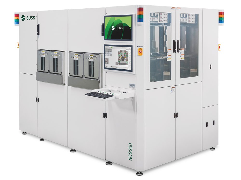
The ACS200 Gen3 TE for 200 mm wafers is the further advanced version of the ACS200 Gen3 with higher throughput, future-ready options and operation comfort for advanced packaging applications of tomorrow. Higher throughput, increased user comfort Advanced automation, unmatched configuration flexibility: The ACS200 Gen 3 TE combines innovative features and stable processing making it the platform of choice for transferring R&D results into robust high volume manufacturing. Extended Flexibility Experience manufacturing flexibility due to configurable 3M, 5M, and 6M frames and 100 to 200 mm wafer processing with fast tooling changeover. The scalable, field-upgradable cluster architecture, 2 or 4 I/O stations or a continuous run load port plus market-leading scheduler properties deliver maximum productivity and stable results. Increased Productivity The ACS200 Gen3 TE boosts throughput by more than 30% compared to the ACS200 Gen3. Up to Six spinner modules and the introduction of In-Motion Centering (IMOC) streamline the handling process, thus eliminating a separate alignment step for faster, more efficient processing. Comfortable Operation Designed with the operator in mind: the ACS200 Gen3 TE includes two standard monitors and easily accessible media cabinets for better usability and convenience. Additionally, lifted EMO (Emergency-off) buttons prevent accidental activation, while a modern white color scheme improves the work environment. Improved Media Flow Accuracy New features for process stability and flexibility: A precise flow controller ensures more accurate media dispensing, while a new combined developer module handles both aqueous and solvent processes thus eliminating the need for separate modules. Effortless Handling of Challenging Wafers Warped, ultra-thin or stacked wafers – the special designed tooling with sophisticated chuck and bowl design plus end effectors ensures secure handling of all kinds of substrates while meeting all standards for protection against electrostatic discharge (ESD). Key Features of ACS200 Gen3 TE 200mm Coater & Developer Benchmark for ultimate performance State-of-the-art technology plus easy handling: the ACS200 Gen3 TE allows for accurate, flexible and robust operations and delivers ultimate throughput. High-Precision Thin Resist Processing The perfect fit for Redistribution Layer (RDL) and Microelectromechanical System (MEMS) application: handle thin resist applications supporting viscosities from very low (<100cp) to high (<5,000cp) and achieve film thicknesses between thin (<100nm) and thick layer (<10um). Thick Resist Processing for Advanced Packaging Engineered for Advanced Packaging applications, you can achieve film thicknesses including passivation from <5µm to <250µm. The ACS200 Gen3 can process any resist type with a viscosity range from very low (<100cp) to very high (<20,000cp) Versatile Develop Processes Get maximum flexibility to develop thin and thick resists or polyimide with a variety of media, from TMAH to solvent-based solutions. With different nozzle types and N2 purge drying options, you achieve precise control and flawless results every time.
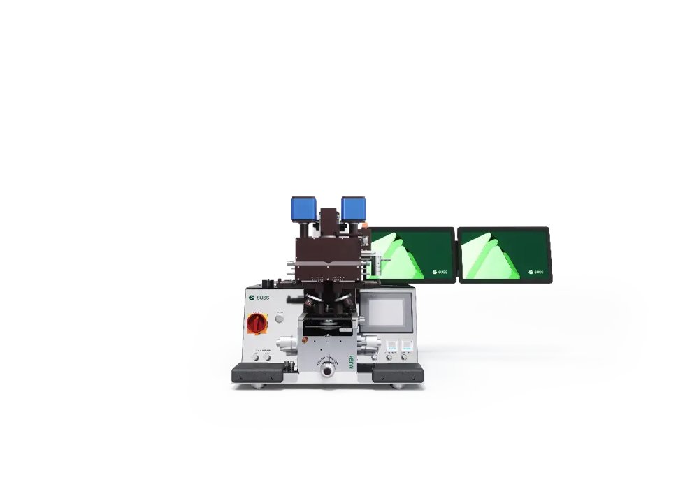
Manual Mask Aligner The MJB4 is the ideal manual mask aligner for research and small-volume production. Compact, easy to use, and cost-efficient, the system is equipped with reliable, high precision mask alignment and high resolution printing capability for substrates and pieces up to 100 mm. Empowering research with precision and versatility The MJB4 combines proven lithography performance with process versatility for research and low-volume production. Supporting fragile materials and UV-NIL, the system´s sub-micron resolution and quick substrate changeovers make it a cost-efficient solution. Precision for Every Process Precise alignment and high-quality results for a wide range of applications, flexible exposure modes - including soft, hard, and vacuum - combined with high-resolution optics and SUSS microscopes deliver resolutions ranging from 2 µm down to less than 0.5 µm. Cost-Efficient by Design Purpose-built for universities and small-scale production, the MJB4 combines affordability with stabel performance. Its compact design, fast setup, configuration upgrades and reliable operation ensure a quick return on investment making the system a cost-efficient and flexible choice for agile R&D labs. Versatile Pioneer in Lithography As one of the first mask aligners, the MJB4 platform set industry standards in research and low-volume manufacturing. Equipped with state-of-the-art technology and multiple configuration modes, the system remains the reference tool for small substrates and pieces worldwide. Operator Ease & Comfort With an intuitive interface and straightforward controls, the MJB4 is designed for exceptional user friendliness. Automated Wedge Error Compensation (WEC) and integrated simulation software for lithographic processes simplify operation, minimize setup time, and guarantee optimal processing for best results. Key Features of MJB4 Mask Aligner The MJB4 delivers reliable lithography through MO Exposure Optics ®, multiple exposure modes, and modular upgrades. With sub-micron resolution and UV-NIL options, it provides a flexible technical foundation for advanced R&D and pilot production. Excellent Light Uniformity With micro-lens plates, MO Exposure Optics ® provides light uniformity over the full exposure field and a larger process window, leading to higher yields. The telecentric illumination decouples the exposure light from the lamp source, saving on setup and maintenance time while ensuring consistent results throughout the lamp's lifespan. Precise Alignment, Broad Flexibility The MJB4 is equipped with a high-precision alignment stage, offering top-side or IR alignment and a choice of Singlefield or Splitfield microscopes for clear pattern recognition and precise results. With optional upgrades for nonstandard substrates or UV-nanoimprint lithography, the system is ideal for MEMS, optoelectronics, hybrids, and fragile III-V materials. Adaptable Tooling The MJB4 grows with your research needs: with a large tooling library that can handle pieces from 5x5 mm up to 100 mm wafers in various shapes and thicknesses up to 4 mm, the MJB4 provides maximum flexibility. Specialized tooling is also available for handling odd-shaped substrates and other non-standard pieces.
CATEGORY
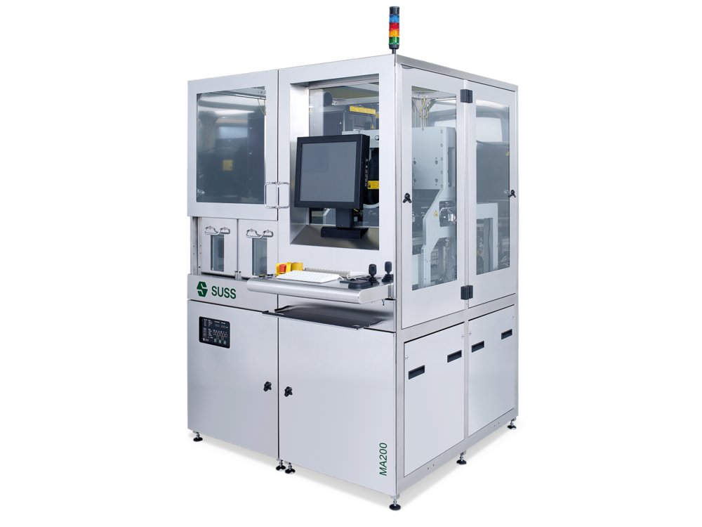
Fully automated Mask Aligner The MA200 Gen3 is engineered for high-volume automated production of wafers and square substrates up to 200mm. Combining innovative alignment technologies with intelligent automations, it's the system of choice for micro-electromechanical systems (MEMS), radio frequency (RF) and power devices. High-volume lithography with sub-micron accuracy Precision, productivity, and flexibility in one tool: MA200 Gen3 features innovative technology for high accuracy, while flexible process modes and automation secure yield and efficiency for MEMS, 3D patterning, and advanced packaging applications such as 3D integration, fan-out, bumping, compound semiconductors, and image sensors. High Alignment Precision For demanding overlay requirements, the MA200 Gen3 features DirectAlign ® with industry-standard PatMax. Using live images instead of stored patterns, it achieves top-side alignment accuracies down to 0.5 µm ensuring exceptional process stability and repeatability ideal for high-volume applications. Unique Illumination Optics SUSS´ MO Exposure Optics ® delivers uniform light distribution with unmatched stability. Its plug-and-play design allows fast switching between HR and LGO modes, while telecentric illumination broadens the process window. With customizable filters and downsizing kits for smaller wafers, the system adapts quickly to diverse production requirements. Versatile Exposure for Sub-Micron Precision The MA200 Gen3 supports multiple exposure modes to match every process need. Proximity lithography enables fast, cost-effective microstructures down to 3.5 µm, while contact and vacuum exposure achieve sub-micron precision below 0.8 µm. Whether for MEMS, packaging, or image sensor applications, this versatility ensures both flexibility and high resolution without compromising throughput. Automated Mask Management The integrated mask library stores and manages multiple photomasks in a controlled environment. Automated selection and activation of the correct layer reduce operator errors and save valuable process time. This streamlines production, increases productivity, and ensures reliable, error-free operation even in high-volume manufacturing. Performance and Yield The SUSS compensation system ThermAlign ® stabilizes chuck and mask temperatures during processing, counteracting thermal run-out in real time. By adapting to changing process conditions, it ensures consistent overlay accuracy and higher yield across long production runs. The mask aligner for advanced packaging Key Features of MA200 Gen3 Mask Aligner Engineered for high-volume environments, the MA200 Gen3 combines precision alignment, advanced optics, and versatile handling to deliver stable, reproducible results across diverse lithography and packaging processes. DirectAlign® Precision Top-side alignment accuracy of 0.5 µm with DirectAlign ®, the SUSS enhanced functionality for structure detection software delivers outstanding overlay performance for demanding production requirements. Flexible Exposure Modes Down to <0.8 µm The MA200 Gen3 adapts to every resolution needed – from fast proximity lithography to sub-micron vacuum contact. It enables structures down to 3.5 µm on 200 mm wafers and <0.8 µm in vacuum mode for maximum flexibility and precision. Secure Handling of Fragile Substrates Interchangeable tooling ensures safe processing of fragile, warped, or ultra-thin wafers down to 50 µm. Edge handling carriers protect double-sided structures, securing yield and throughput in advanced applications.
CATEGORY
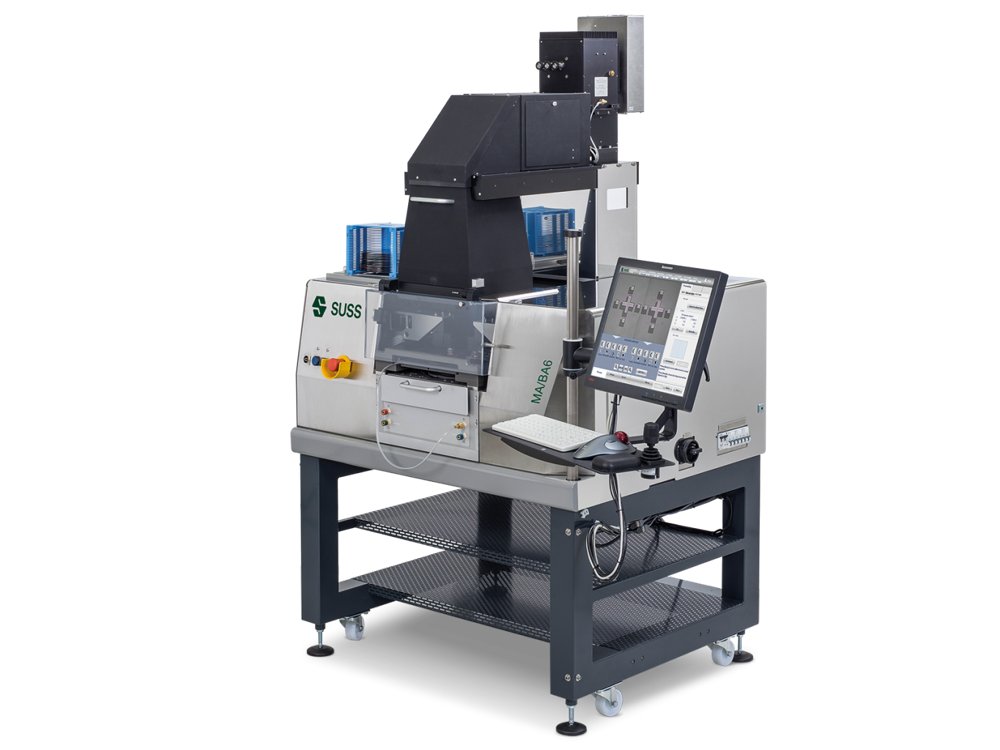
The MA/BA Gen4 series represents two platforms for semi-automated mask aligner and imprint processing for both standard or high-end applications. Combining proven SUSS lithography technology with new automation and ergonomic features, the system ensures stable performance, enhanced safety, and user-friendly operation for research, pilot production, and demanding process environments. Your Benefits Designed for intuitive operation and ergonomic ease, the MA/BA Gen4 reduces operator effort and ensures process consistency across MEMS, packaging, and imprint applications. State-of-the-Art Technology Optimal results for advanced lithography and imprint processes across a wide substrate range: latest alignment techniques, the unique SUSS exposure concept and MO Exposure Optics ® deliver the highest level of alignment and mechanical precision, superior resolution plus environmental sustainability and energy efficiency. Outstanding Versatility Available as MA/BA6 Gen4 and MA/BA8 Gen4 for standard processes, or MA/BA Gen4 Pro for advanced and high-end applications, the system delivers excellent, reproducible results from microstructures to nanoscale imprinting. High automation and SMILE technology enable seamless application exploration and scale-up on one versatile platform. Operator Ease & Comfort The MA/BA Gen4 series features clear interfaces, guided workflows, and intuitive controls. The ergonomic recipe editor, sophisticated data logging and the ability to assign user rights reduce operator effort, minimize errors, and shorten training time ensuring efficient, comfortable operation even during extended shifts. Compact Design, Scalable Performance The scalable bridge between research and production: Identical process modules and software interfaces allow direct process transfer to SUSS’s automated platforms, enabling efficient scale-up and reducing qualification effort in high-volume environments. Key Features of MA/BA Gen4 Series Equipped with MO Exposure Optics ® and SUSS latest imprint technologies, the MA/BA Gen4 series delivers optical excellence, precision alignment, and superior resolution. Its modular design supports advanced packaging, MEMS/NEMS, 3D integration, compound semiconductors, LED, micro-optics, AR, and optoelectronics. Excellent Light Uniformity MO Exposure Optics ® with telecentric illumination provides superior light uniformity and process stability. Exchangeable aperture plates and customizable illumination deliver flexibility and yield gains for a wide range of lithography and imprint applications. Highest Level of Alignment Precision The MA/BA Gen4 series offers top-side, bottom-side, and infrared alignment to handle diverse substrate configurations. Optional DirectAlign ® technology achieves 0.5 µm overlay accuracy through live image detection, ensuring reliable alignment even for complex structures, multilayer stacks, and challenging process conditions. Excellent Resolution and Pattern Fidelity Resolution down to 0.8 µm across hard, soft, or vacuum contact modes and a new energy-efficient lamp house set new full-field lithography benchmarks. Integrated simulation with custom SUSS optical models enables process visualization, quantitative predictions, and parameter optimization for optimal results.
CATEGORY
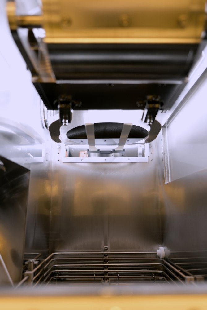
Sustainable wafer cleaning with hybrid approach The GT200 is an eco-friendly manufacturing solution dedicated to wafer cleaning and stripping processes. From photoresist removal and surface activation to high-quality final cleaning, GreenTec Solutions brings complementary process capabilities together in one configurable platform. By consolidating these capabilities, the GT200 helps reduce tool fragmentation, simplify process flows, and establish a more consistent foundation for efficient and reliable production. Dedicated wafer cleaning platform built on proven photomask processing expertise Eliminate the need for hazardous substances by combining greener process media with SUSS hybrid stripping approaches. Lower your EHS Exposure GT200 reduces the use of hazardous substances by enabling greener process media and alternative stripping approaches. This helps lower EHS exposure, simplifies waste handling, and supports internal sustainability targets while maintaining reliable cleaning performance Reduced process complexity By consolidating several cleaning and stripping steps into one flexible tool concept, the GT200 reduces wafer transfers and toolset complexity. This supports more stable process flows, fewer interfaces, and improved operational efficiency across the line. Faster learning cycles Designed for low-volume manufacturing, the GT200 enables controlled experimentation, process tuning, and recipe development. Together with SUSS process expertise, customers can shorten adoption time and move faster from evaluation to stable production. Lower cost of ownership SUSS GT200 supports TCO reduction by lowering chemistry consumption, reducing hazardous waste, and simplifying safety and abatement requirements. Efficient media use and modular process integration help fabs manage resources more effectively. Scalable process transfer A modular platform concept and joint evaluation approach support the transfer of process know-how from pilot lines and qualification into high-volume manufacturing. This enables customers to build confidence early and scale with a consistent process strategy. Benchmark for sustainable cleaning performance Key Features of the GT200 Advanced green cleaning and stripping technologies designed to reduce chemical impact, improve process control, and support reliable manufacturing. TurbulenStrip technology TurbulenStrip uses a dynamic single-wafer wet process with a strip in soak bath and exclusive green fluids. The locally turbulent flow creates high forces at the substrate surface, supporting efficient resist, polymer, descum, and post-etch cleaning while reducing cross-contamination, all while saving half consumption and disposal compared to DMSO. CrustBuster UV residue removal CrustBuster applies SUSS patented in-situ UV technology to break down organic materials directly at the substrate surface. This hybrid approach enables stripping with significantly reduced chemical use and supports gentle processing for sensitive structures and sustainable manufacturing goals. Spin-Rinse-Dry for efficient final cleaning performance The GT200 supports up to 200 mm wafers with up to 45 wafers per hour and a particle removal efficiency of 99 % for particles 100 nm. Its compact footprint and modular configuration make it suitable for controlled learning, qualification, and low-volume production.
CATEGORY
