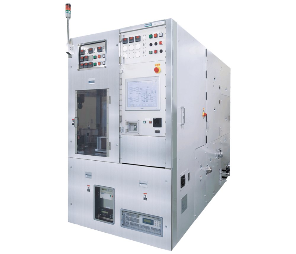
By SAMCO Inc.
⌀4″ Open Load LSCVD® none Open load system up to ø100 mm (4") The PD-100ST is a low-temperature (80 ~ 400°C), high-rate (>300 nm/min) plasma-enhanced CVD system for R&D. Samco’s unique liquid source CVD system uses self-bias deposition techniques and a liquid TEOS source to deposit SiO2 films with low stress, from thin films to extremely thick films (up to 100 µm). With its sleek, compact design, the PD-100ST requires minimal cleanroom space. Key Features & Benefits - Processing up to ø100 mm (4″) - Cathode coupled self-bias deposition techniques enables high-rate (>300 nm/min) deposition of low-stress films - By low temperature deposition, films can be deposited on top of plastic surfaces - Excellent step-coverage of high aspect ratio structures - Control of refractive index by using germanium, phosphorus, and boron liquid precursors - With its sleek, compact design, the PD-100ST requires minimal cleanroom space Applications - Deposition of protective films over plastic materials - Deposition of the insulating film on via sidewalls for 3D LSIs - Fabrication of optical waveguides (fiber core/cladding) - Fabrication of masks for use in the production of micromachines - Coverage of high aspect ratio structures such as MEMS devices - Temperature compensation film and passivation film for SAW devices Papers Lee, M. L., Wang, S. S., Yeh, Y. H., Liao, P. H., & Sheu, J. K. (2019). Light-emitting diodes with surface gallium nitride p–n homojunction structure formed by selective area regrowth. Scientific reports, 9(1), 1-7. https://doi.org/10.1038/s41598-019-40095-7 Nishijima, T., Shimizu, S., Kusano, K., Kudo, K., Furuta, M., Kusuda, Y., … & Tsunoda, I. (2020). Au induced lateral crystallization of amorphous Ge with stress stimulation at 130°C. AIP Advances, 10(5), 055306. https://doi.org/10.1063/5.0004326 Cheng, X., Hong, J., Spring, A. M., & Yokoyama, S. (2017). Fabrication of a high-Q factor ring resonator using LSCVD deposited Si3N4 film. Optical Materials Express, 7(7), 2182-2187. https://doi.org/10.1364/OME.7.002182
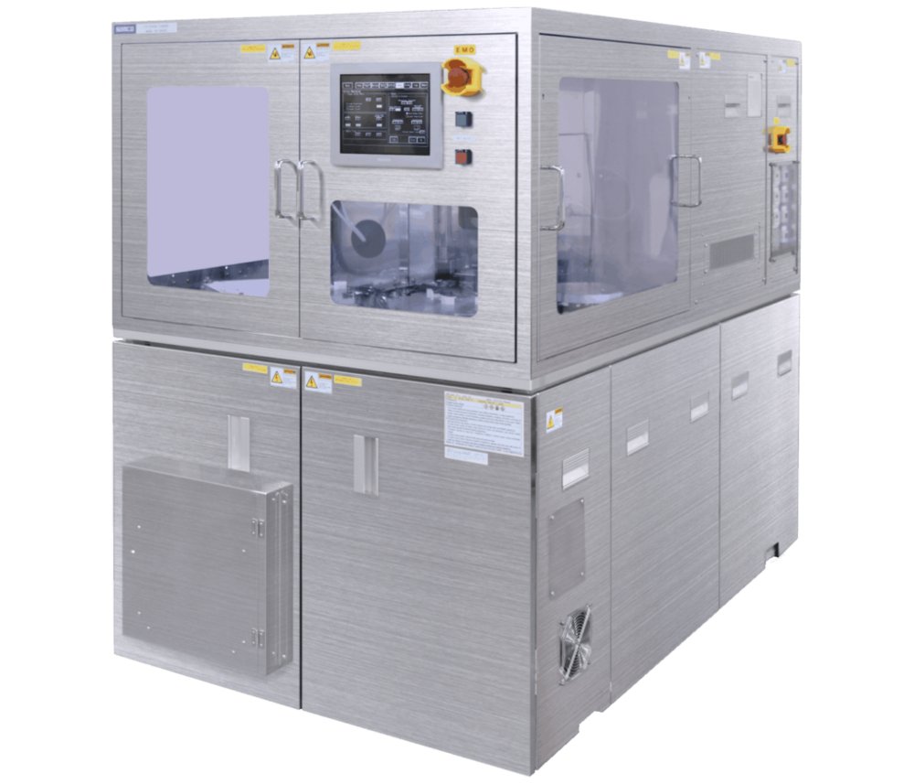
Samco’s UV ozone cleaning systems offer a sophisticated method for surface treatment by combining ultraviolet (UV) irradiation, ozone, and stage heating. This powerful, yet gentle process effectively removes organic contaminants from a wide range of substrates, including silicon, glass, and compound semiconductors such as GaN, SiC, GaAs, and InP. Available in compact benchtop and cassette-loading configurations, Samco’s UV ozone cleaners cater to both R&D and mass production environments, ensuring versatility and efficiency. With systems designed to handle a variety of materials, UV ozone cleaning is an ideal solution for those seeking a dry, non-invasive method for substrate preparation and contamination removal. UV ozone treatment works by utilizing both 185 nm and 254 nm UV light wavelengths. The 185 nm UV light dissociates molecular oxygen into atomic oxygen, which reacts with ozone to form highly reactive singlet atomic oxygen. This powerful oxidant interacts with the substrate surface to remove organic residues, while the 254 nm UV light dissociates ozone, further enhancing the oxidation process. Additionally, stage heating plays a crucial role by accelerating ozone dissociation at higher temperatures, increasing the concentration of singlet atomic oxygen and improving cleaning efficiency. This process results in the removal of organic contaminants without causing damage to the substrate, making it particularly useful for sensitive materials like semiconductor wafers. The UV ozone cleaning systems also feature an ozone decomposition unit and automatic nitrogen purging for enhanced safety, ensuring a completely dry, chemical-free treatment. COP samples treated with UV Ozone and stage heating, along with ozone flow, maintained stable hydrophilic surfaces for 180 days, demonstrating the long-term effectiveness of UV Ozone treatment compared to oxygen plasma. Ozone generator provides a higher ozone concentration and sample stage heater allows process temperature control up to 300°C. These features increase the reactive oxygen species during the process and improve the etch rate.
CATEGORY
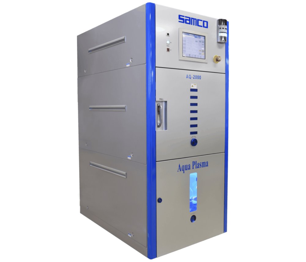
406 x 413 mm Open Load Aqua Plasma™ none Scalable System for Batch Processing The AQ-2000 is a scalable Aqua Plasma® cleaning system designed for production-scale operations. With H₂O as the process gas, it offers safe, eco-friendly treatments like reducing metal oxide films, cleaning organic stains, resin bonding, and superhydrophilization. Equipped with multiple shelves, it supports batch processing for samples up to 406 x 413 mm. Key Features & Benefits - Safe reduction and cleaning of metal oxide films with Aqua Plasma® technology. - Built-in automatic control system for water vapor generation and supply. - Space-efficient design suitable for production environments (762 mm (W) x 1135 mm (D)). Applications - Reduction, cleaning, and modification of silver and copper electrodes. - Room-temperature bonding of dissimilar materials. - Surface modification of resins, including superhydrophilization. Options - Quartz cover (to prevent spattering of powered electrodes) Processes Reduction of copper in electronic device applications Silver electrode reduction for LED packages Superhydrophilization of COP COP bonding at room temperature
CATEGORY
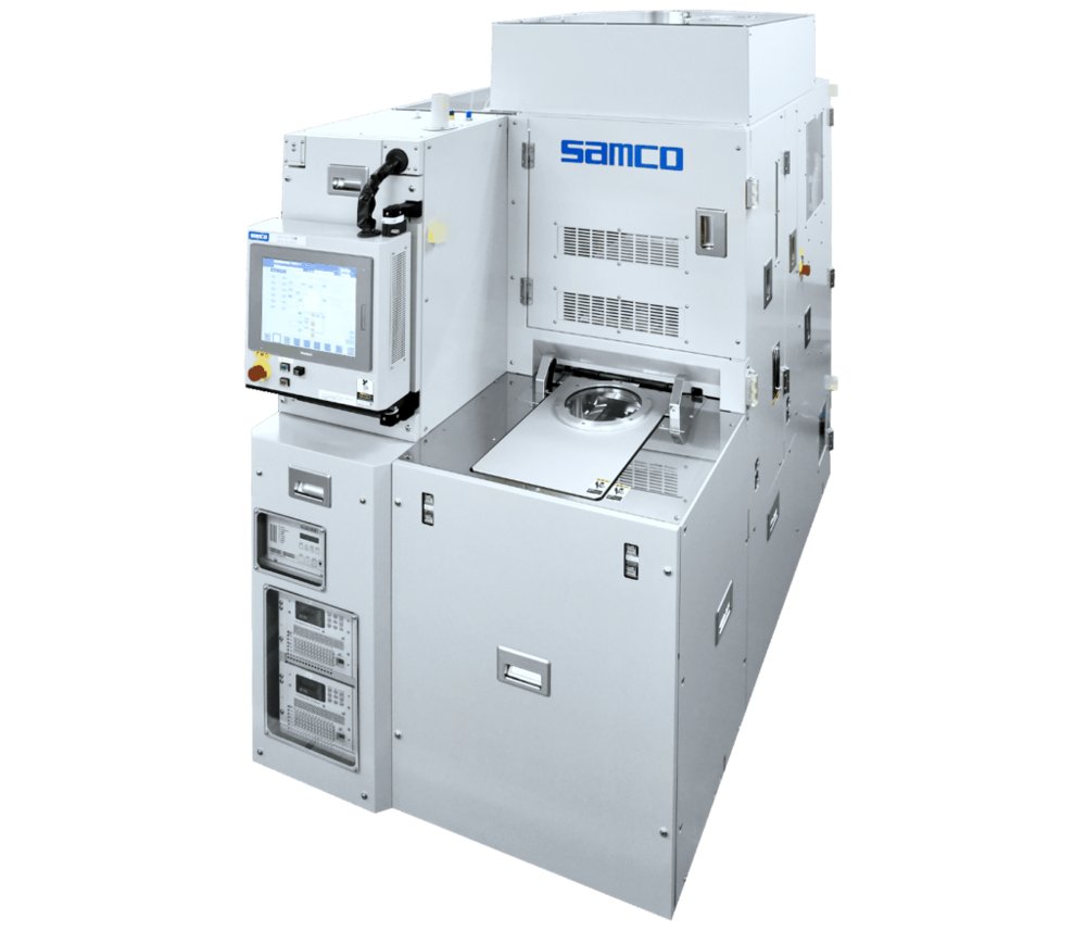
Atomic Layer Etching System RIE-800iP-ALE ⌀8″ Load Lock ALE none Precise depth control The RIE-800iP Atomic Layer Etching (ALE) system is an advanced and versatile tool designed for precise and controlled etching processes at the atomic scale. Equipped with cutting-edge technology, the RIE-800iP ALE enables researchers and engineers to achieve atomic-level precision in etching various materials. The system employs the Atomic Layer Etching method, ensuring highly uniform and reproducible results. Key Features & Benefits - Robust, Fast-Switching Gas Input Valve: Ensures stable and reliable performance for ALD and ALE processes. - New ICP Source HSTC™ (Hyper Symmetrical Tornado Coil): Efficiently applies high RF power (2 kW or more) for excellent stability and uniformity. - High Flow Exhaust: Directly connected to the reaction chamber, supporting a wide process window from low flow/pressure to high flow/pressure. - Endpoint Monitoring: Compatible with interferometric and emission spectroscopic methods for precise film thickness detection. - Easy-to-Maintain Design: Integrated TMP and high-frequency power supply allow for straightforward replacement and maintenance. Applications - Recess etching for GaN HEMT - p-GaN/AlGaN high selectivity ratio etching - 2D materials etching - Photonic crystal etching - Low rate and low damage etching Options - Interferometric endpoint monitor High-precision endpoint detection is possible, and the etching depth can be controlled to the desired depth. Processes High selectivity etching ALE of GaN Control of micro-loading effects ALE of SiO2 Papers Development of Atomic Layer Etching (ALEt) for GaN-based materials Congying You, C. Mannequin, G. Jacopin, T. Chevolleau, C. Durand, et al.. Development of Atomic Layer Etching (ALEt) for GaN-based materials. International Workshop on Nitride Semiconductors, Nov 2018, Kanazawa, Japan. hal-02008012 Comparative study of two atomic layer etching processes for GaN Cédric Mannequin, Christophe Vallée, Katsuhiro Akimoto, Thierry Chevolleau, Christophe Durand, et al.. Comparative study of two atomic layer etching processes for GaN. Journal of Vacuum Science & Technology A, 2020, 38 (3), pp.032602. ff10.1116/1.5134130. hal-02917577
CATEGORY
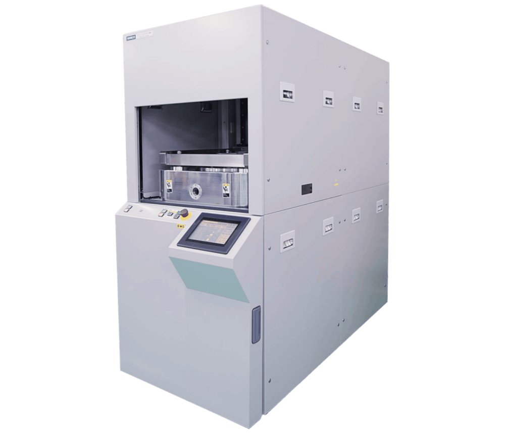
Samco offers reliable and durable Reactive Ion Etching (RIE) systems for R&D and production customers. Our benchtop compact RIE etcher is a suitable tool for academic device research and die deprocessing for IC failure analysis. Samco's open load RIE systems and load lock RIE systems have a wide process window for plasma etching of various materials (silicon, dielectrics, compound semiconductors, metals, polymers and photoresist). The cassette loading RIE systems improve process throughput for device fabrication.
CATEGORY
