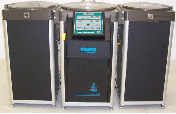
As devices become smaller and more sophisticated, the art of Failure Analysis has become increasingly challenging. Trion Technology is pleased to offer a new type of processing tool that combines both dielectric, and metal etching to allow rapid de-processing using complimentary processes. The Minilock-Phantom Duo is designed to supply failure analysis laboratories with state-of-the-art plasma etch capability using single wafers, dies or parts using both fluorine and chlorine based chemistries. The Minilock-Phantom Duo allows two independent process modules to be coupled to a Minilock. This increases research capability by not exposing samples to atmosphere between layers. The system can be configured for 8 inch, 300mm, or 450mm chucks in a footprint that is the same as a typical single chamber system from our competitors. Any combination of PR Strip, RIE, PE, ICP or DRIE modules is possible.
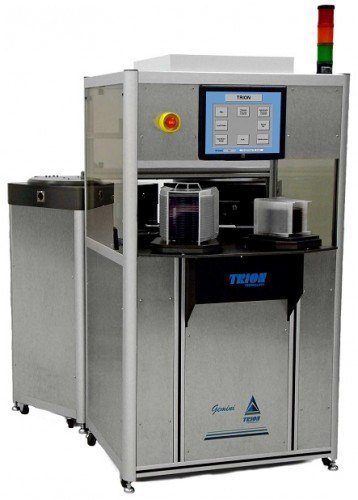
Gemini Multi-Chamber Photoresist Stripper The Gemini is a compact multi-chamber, high throughput photoresist stripping system that is designed specifically for the demands of today’s production fabs.This versatile and affordable system can be configured with a 200mm or 300mm chuck. As required by application, this system can incorporate a microwave source (which is both reliable and free from typical microwave tuning problems) or ICP technology. By employing ICP, microwave and RF bias power difficult to remove layers of resist can be removed at low temperatures. - Etch rates up to 6um/min - High throughput - Low plasma damage - Automatic tuning - 100mm to 300mm wafers - Small footprint - Competitively priced Inductively Coupled Plasma (ICP) Option: High Rate and Low Damage Photoresist Stripping is a critical necessity in modern semiconductor manufacture. As more and more masking steps and more sensitive devices have come into use, “plasma downstream ashing” has become the primary method of resist removal. The Trion Gemini Photoresist Stripper incorporates a downstream Inductively Coupled Plasma (ICP) to provide the high rate and uniform removal this application requires. The Trion Gemini system was specifically designed for production Photoresist Descum and Stripping. This extremely reliable system provides a compact and inexpensive solution to this application. Single-Chamber Option Applications: MEMS, Compound Semiconductor, Advanced Packaging.
CATEGORY
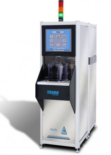
The cost of new photoresist stripping systems has escalated to unreasonable levels. Trion has solved this critical problem. The Apollo Stripper is a compact, inexpensive, and versatile system which can be configured for a 200mm or 300mm Chuck. By employing RF bias power, difficult to remove layers of resist can be removed at low temperatures. As required by application, this system can incorporate a microwave source (which is both reliable and free from typical microwave tuning problems) or ICP technology. - Etch rates up to 6um/min - High throughput - Low plasma damage - Automatic tuning - 100mm to 300mm wafers - Small footprint - Competitively priced Inductively Coupled Plasma (ICP) Option: High Rate and Low Damage Photoresist Stripping is a critical necessity in modern semiconductor manufacture. As more and more masking steps and more sensitive devices have come into use, "plasma downstream ashing" has become the primary method of resist removal. The Trion Apollo Photoresist Stripper incorporates a downstream Inductively Coupled Plasma (ICP) to provide the high rate and uniform removal this application requires. The Trion Apollo system was specifically designed for production Photoresist Descum and Stripping. This extremely reliable system provides a compact and inexpensive solution to this application. Applications: MEMS, Compound Semiconductor, Pilot Line Production.
CATEGORY
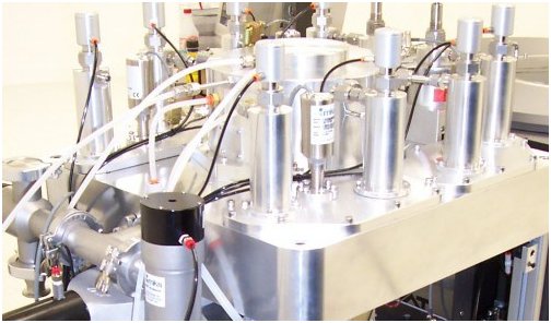
Atomic Layer Deposition (ALD) is a new cutting edge technology for the Semiconductor Industry. It provides super high-density films that are extremely uniform with exceptional step coverage. The Minilock ALD system has the capability to grow Atomic Layer Deposition films in Thermal and Plasma Enhanced modes (PEALD). It has the industry's smallest footprint and lowest cost of ownership.The system is available for wafers up to 300mm in diameter. ALD is a thin-film deposition technique based on the sequential use of a gas-phase chemical process and/or plasma processes (PEALD). The majority of ALD reactions use two chemicals called precursors and reactants. The precursor adsorbs onto the surface of the material and the reactant is added thereafter, one at a time in a sequential, self-limiting, manner. By keeping our core components the same, it is very easy to scale to a production cluster platform. Standard processes have been developed for various materials. This is backed by over 25 years' experience in rapid process development. Features: - Inductively Coupled Plasma Source (ICP, PEALD) - Biased electrode - Vacuum loadlock - 4 Precursor entry points - Turbo pump - Programmable Logic Controller (PLC) and touch screen control - SEMI S2 and CE compliant
CATEGORY
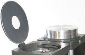
The Minilock-Orion is a Plasma Enhanced Chemical Vapor Deposition system with a vacuum loadlock that produces production-quality films on a compact platform. By adding a loadlock, dopants can be used on the PECVD films. The unique reactor design produces low stress films with excellent step coverage at extremely low power levels. The system meets all safety, facility and process requirements within the laboratory and pilot line production environments. The Minilock-Orion has many standard features not typically found on a system so reasonably priced, which is why many users worldwide have made it their PECVD system of choice. Applications: MEMS, Solid State Lighting, Failure Analysis, Research & Development, Pilot Line. Toxic/Pyrophoric PECVD Processes Films Deposited: - Oxides - Oxynitrides - Nitrides - Amorphous Silicon - Silicon Carbide Process Gases: - 100% Silane - Ammonia - TEOS - Diethylsilane - Nitrous Oxide - Oxygen, Nitrogen - Trimethylsilane - Methane
CATEGORY
