We have nanopore chips (pore diameter 50nm to 10μm) suitable for measuring viruses and proteins.
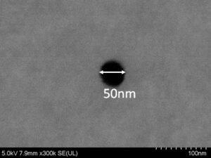
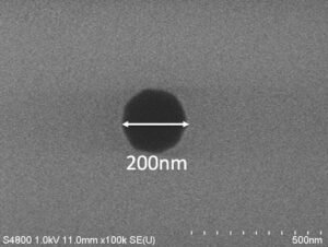
tei Solutions offers 100mm, 150mm, 200mm, and 300mm blanket and pattern wafers for material and tool evaluation including: - Nano Pore Pattern - Line and Space - Hole Pattern - Al Pad wafers - Cu Pad wafers - Others – Please contact us for special structures or materials. Customers can utilize their own mask set if the clean level is acceptable. Nano Pore Pattern Examples Pore Size:50nm Pore Size:200nm Pore Size:10μm φ300mm Patterned Wafer Examples L/S=260/40nm, SiO Etch Pitch=300nm(6.5:1) AR=approx.4.5(Depth=190nm) X-SEM L/S=100/100nm, Si Etch Pitch=200nm(1:1) AR=approx.23(Depth=2300nm) X-SEM TOP CD(Cu)=approx.80nm, Low-k Etch Pitch=160nm(1:1) Depth=180nm X-SEM Si L/S Etch Si Substrate Etching (Top)L/S=150nm/150nm, Pitch=300nm AR=approx.18(Depth=2770nm) X-SEM Si Hole Etch (Top)Hole=φ1000nm Depth=10000nm X-SEM SiO2 L/S Etch SiO film etching (Top)L/S=180nm/120nm, Pitch=300nm Depth=2700nm X-SEM φ300mm Blanket Wafer Examples Diffusion – SiO – Thermal Oxide – 1〜500 nm CVD – SiO – LP-TEOS – 10〜300 nm CVD – SiO – P-TEOS – 30〜2000 nm CVD – SiO – P-SiO2 – 20〜500 nm CVD – SiO – HDP – 30〜1,000 nm CVD – SiN – LP-Si3N4 – 10〜100 nm CVD – SiN – P-Si3N4 – 20〜1000 nm CVD – Si – Poly-Si – 20〜500 nm CVD – Si – amorphous-Si – 20〜500 nm CVD – Si – Doped-Si – 20〜500 nm CVD – SiOC – P-SiOC – 30〜400 nm CVD – SiCN – P-SiCN – 10〜200 nm CVD – AlO – ALD-Al2O3 – 2〜10 nm CVD – HfO – ALD-HfO2 – 2〜10 nm CVD – W – CVD-W – 50〜600 nm CVD – TiN – CVD-TiN – 5〜30 nm CVD – Ti – CVD-Ti – 2〜20 nm Sputter – TiN – PVD-TiN – 5〜30 nm Sputter – Ti – PVD-Ti – 2〜20 nm Sputter – Al(Cu) – PVD-Al(Cu) – 100〜1000 nm Sputter – TaN – PVD-TaN – 5〜50 nm Sputter – Ta – PVD-Ta – 8〜80 nm Sputter – Cu – PVD-Cu – 15〜200 nm Plating – Cu – Cu Plating – 300〜5000 nm Coating – Resist – for ArF – Contact Us Coating – Resist – for KrF – Contact Us Coating – Resist – for i-Line – Contact Us Coating – BARC – for KrF – Contact Us Coating – SOC – for Imm-ArF – Contact Us Coating – SOG – for Imm-ArF – Contact Us Should you require other types or thicknesses of film, please do not hesitate to contact us. φ200mm – Patterned Wafer Examples - High Aspect ratio Si hole pattern, Hole size 200nm, AR=40. - Al Pattern, VIA size 800nm, - Al Pattern, 0.35micron - Deep Si hole, Hole size 10um minimum, depth 50um maximum φ200mm – Blanket Wafer Examples - SiGe Epi on Si, Ge content maximum 20% φ150nm – Patterned Wafer Example - Al Pattern, 0.5micron φ100mm - Patterned Wafer Example - Al Pattern, 0.8micron
CATEGORY
