Custom transmission gratings for EUV and higher energy X-ray systems. Our direct-write, fast through-put process allows for high resolution gratings with areas that span several hundred micrometres to millimetres. Various metals can be fabricated on thin membranes of silicon nitride, silicon carbide, or silicon. High Resolution Resolution down to 20 nm half pitch, or 50,000 line pairs/mm. Membrane Options Gratings can be fabricated on silicon or glass substrates. For transmission gratings, available substrates include thin silicon nitride, silicon carbide, or silicon membranes with thicknesses between 50 nm to 1000 nm. The substrates can be chosen to suit your application. High Aspect Ratio High-resolution direct-write patterning allows for custom designs and high efficiency gratings for hard X-ray applications. Gold, nickel, platinum, and tungsten metals with positive and negative-tone patterning are available. Custom Applications Our custom gratings can be used in synchrotron and lab-based systems for a range of applications. Contact us for more details for your specific needs. Gratings Designs Available (custom designs upon request) Device | Material | Thickness | Pitch | Lines/mm | Lines & Spaces / mm | Membrane | Area | Design Energy 500um-80nm-W | Tungsten | 100 nm | 80 nm | 25000 | 12500 | 50-100 nm silicon nitride | 500 μm x 500 μm | 200-1000 eV 500um-80nm-W | Rutheniu | 55-150 nm | 40 nm | 50000 | 25000 | 50-100 nm silicon carbide | 500 μm x 500 μm | 20-1000 eV 1000um-80nm-W | Tungsten | 100 nm | 80 nm | 25000 | 12500 | 50-100 nm silicon nitride | 1000 μm x 1000 μm | 200-1000 eV 500um-50nm-Au | Gold | 150-200 nm | 50 nm | 40000 | 20000 | 50-100 nm silicon nitride or silicon carbide | 500 μm x 500 μm | 200-1500 eV 1000um-50nm-Au | Gold | 150-200 nm | 50 nm | 40000 | 20000 | 50-100 nm silicon nitride or silicon carbide | 1000 μm x 1000 μm | 200-1500 eV 2mm-2um-Au | Gold | 4-5 μm | 4 μm | 500 | 250 | 100-1000 nm silicon nitride or silicon carbide | 2 mm x 2 mm | 3-12 keV 4 mm-2um-Au | Gold | 4-5 μm | 4 μm | 500 | 250 | 100-1000 nm silicon nitride or silicon carbide | 2 mm x 2 mm | 3-12 keV 2 mm-4um-Au | Gold | 6-8 μm | 8 μm | 250 | 125 | silicon or membrane | 2 mm x 2 mm | 8-20 keV Custom grating requests can be made to sales@appliednt.com. We offer a range of membrane and grating materials for EUV, soft and hard X-rays and optical gratings as well as for holography.
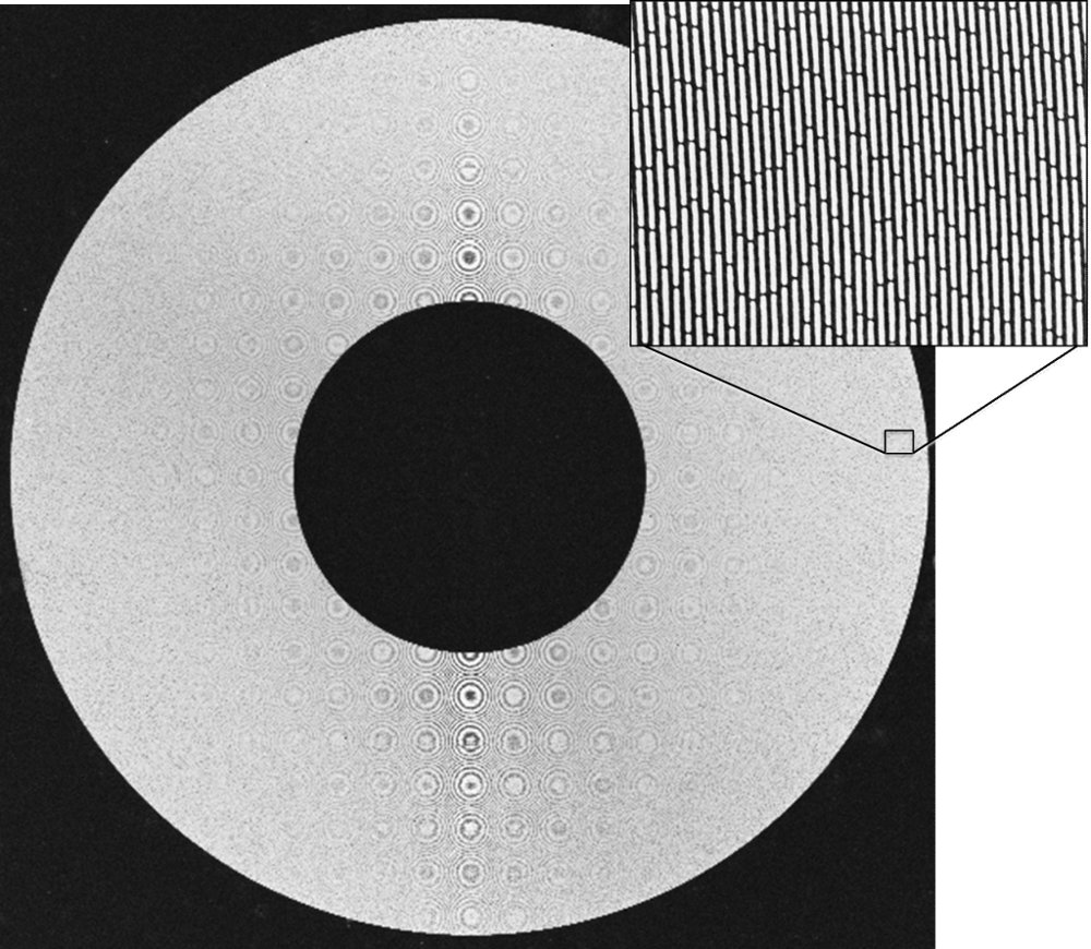
X-rays below 5 keV (<~0.25 nm) are typically classified as soft X-rays, where they are more readily absorbed than higher energy X-rays. Typically, zone plates do not require the same thickness for efficiency and allow for higher resolution imaging. A range of zone plate options for soft/tender X-Rays are available for specific requirements. (Custom Designs Available) Device | Outer Zone Width ΔR n (nm) | Thickness (µm) | Outer Diameter (µm) | ( of zones) E/ΔE Limit | ~ Focal Length(µm) SZP‑90um‑15nm | 15 | <0.07 | 90 | 1514 | 325 SZP‑120um‑15nm | 120 | 2019 | 433 SZP‑200um‑18nm | 18 | <0.15 | 200 | 2797 | 868 SZP‑270um‑18nm | 270 | 3775 | 1172 SZP‑320um‑18nm | 320 | 4473 | 1389 SZP-200um-25nm | 25 | <0.24 | 200 | 2007 | 1207 SZP‑250um‑25nm | 250 | 2509 | 1510 SZP-300um-25nm | 300 | 3010 | 1811 SZP-360um-25nm | 360 | 3612 | 2173 TZP‑160um‑50nm | 50 | <0.75 | 160 | 801 | 1934 TZP‑280um‑50nm | 280 | 1401 | 3384 TZP‑750um‑200nm | 200 | <0.75 | 750 | 938 | 36292 TZP‑1250um‑200nm | 1250 | 1563 | 60487 For estimated efficiency of zone plate, please see our online calculator at www.appliednt.com/zpcalc
CATEGORY
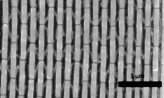
Zone plate efficiency for binary zone plates requires high aspect ratio structures which can survive high flux imaging systems. The “Oxide Interlock” option creates small interconnecting channels between metal zone of silicon dioxide which is transparent to hard X-rays and does not swell or distort, even when not under vacuum. These have been shown to significantly increase the zone plate efficiency and lifetime.
CATEGORY
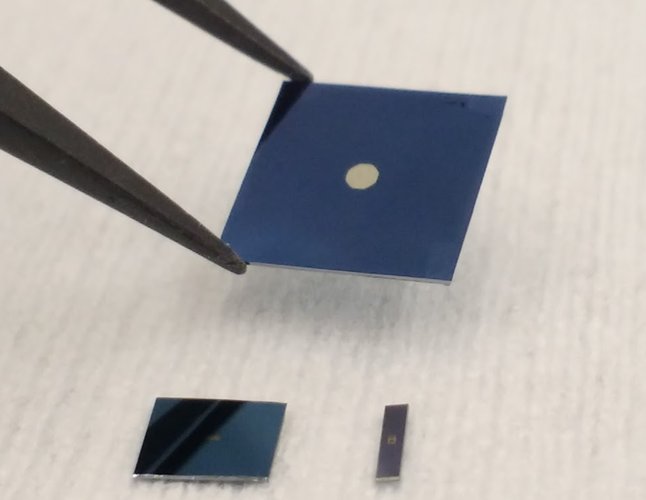
Our standard frame size is 5 mm x 5 mm. We also offer custom frame sizes. Membrane thickness can be down to 50 nm and silicon carbide membranes are available for those requiring long-lifetime membranes. Low stress 50 nm silicon nitride membrane Low stress 200 nm silicon carbide membrane Fused Silica Substrate (~500 um thick) Custom chip sizes
CATEGORY