Grat-FET TM: Graphene Field-Effect Transistors. Bluestone’s Grat-FET TM products are state-of-the-art, three-terminal Field-Effect Transistors (FETs) that rely on Bluestone’s exclusive, high-mobility CVD graphene, Grat-M TM. Each Grat-FET TM chip consists of an array of 36 graphene FETs with nine different graphene channel length/width arrangements to accommodate all research and development settings. Graphene FETs are fabricated on a Si wafer covered with a SiO 2 layer, and the high-mobility Grat-M TM graphene is used as the transistor channel. The graphene transistor consists of three terminals: source and drain metal electrodes contacting the graphene channel and a global back gate enabled by the doped Si substrate. These features facilitate the characteristic ambipolar transport behavior of graphene in the Grat-FETs – achieving both n-type and p-type transport when biased with a proper gate voltage at the substrate. As with all Bluestone products, every Grat-FET is tested to ensure our high-quality standards are met. Features & Benefits - High field-effect carrier mobility of 2000 cm 2/Vs or more - Ambipolar transport - Uncovered graphene channel - Small uncontrolled doping - Fabricated on highly-doped Si substrate, which can be used as gate electrode - Individual control of each transistor to be biased or connected externally - Each chip comes with multiple transistors of nine different channel dimensions Technical Specs Device Parameters Back-gate oxide Thermal SiO 2 Back-gate oxide thickness 300 nm Silicon substrate resistivity 0.001-0.005 Ω-cm Number of graphene layers 1 Gate leakage current<0.5 nA (at V BG = 100V) Channel mobility 2000-3000 cm 2/Vs Contact metal thickness 40 – 50 nm Electrical Characteristic Curves (Room temperature, Ambient)
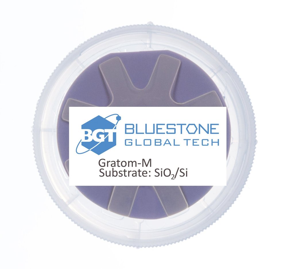
Graphene film coverage 95% with occasional holes and cracks (< 5 %) Monolayer graphene percentage 95% of cracks or holes larger than 3 mm: 0 Average Raman Id/Ig < 5% within domain Average Hall mobility of 2000-4000 cm 2/Vs at n=1e12 /cm 2 Average sheet resistance of 300-600 ohm/sq. Available Sizes: 1cm x 1cm, 2” or 4” wafer Wafer spec: thermal grown 285-nm SiO2 on p-type Si substrate (resistivity <0.005 ohm-cm)
CATEGORY
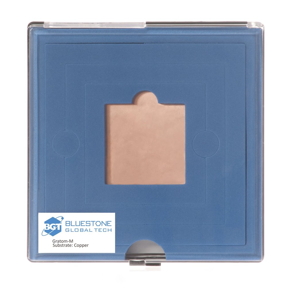
Monolayer percentage 95% Optical transmittance at 550 nm 97% (excl. substrate) Average Raman Id/Ig < 5% within domain Average Hall mobility of 2000-4000 cm 2/Vs at n=1e12 /cm 2 Average sheet resistance of 300-600 ohm/sq. Available Sizes (in 2): 2 x 2, 4 x 4, 8 x 10, 12 x 14 Copper thickness 1mil (25 µm)
CATEGORY
Isolated single graphene domain Large graphene domain (30 – 200 µm) Average Raman Id/Ig < 5% within domain Available Sizes: 2” wafer Wafer spec: thermal grown 285-nm SiO2 on p-type Si substrate (resistivity <0.005 ohm-cm)
CATEGORY
